Element 2
+49 30 641 670 100
Element 1
info@microresist.de
ma-N 1400 series
Negative Photoresists
PVD & Lift-off
Element 25weqwf
ma-N 1400 - Negative Tone Photoresist Series
for Conventional Pattern Transfer and Single-Layer Lift-Off Processes
Unique Features
  • Resists available in a variety of viscosities
  • Aqueous alkaline development
  • Tunable pattern profile: vertical to undercut
  • High wet and dry etch resistance
  • Good thermal stability of the resist pattern
  • Easy to remove
Applications
  • Microelectronics and micro systems technology
  • Mask for lift-off processes
  • Etch mask for semiconductors and metals
  • Well suitable for implantation
  • Mould for electroplating
Resist Film Thickness [µm]
spin coating @ 3000 rpm
Spectral Sensitivity Special Feature
ma-N 1405 0.5 300 - 410nm

i-line - 365 nm

(h-line - 405 nm)

Novolak based resist, thermal stability up to 160°C
for metal evaporation and sputtering
ma-N 1407 0.7
ma-N 1410 1.0
ma-N 1420 2.0
ma-N 1440 4.0
ma-N 402 0.2 300 - 380nm

i-line - 365 nm

Novolak based resist,
thermal stability up to 110°C
for metal evaporation
ma-N 405 0.5
ma-N 415 1.5
ma-N 420 2.0
ma-N 440 4.1
ma-N 490 7.5

Recommended process chemicals:

for ma-N 1400 Series
Thinner: ma-T 1046
Developer: ma-D 533/S (TMAH based)
Remover: mr-Rem 700 (NMP & NEP free), mr-Rem 500 (NMP free), ma-R 404/S (strongly alkaline)
Lift-off: mr-Rem 700 (NMP & NEP free), mr-Rem 500 (NMP free)

for ma-N 400 Series
Thinner: ma-T 1049
Developer: ma-D 331/S, ma-D 332/S (NaOH based), 531/S, ma-D 532/S (TMAH based)
Remover: mr-Rem 700 (NMP & NEP free), mr-Rem 500 (NMP free), ma-R 404/S (strongly alkaline)
Lift-off: mr-Rem 700 (NMP & NEP free), mr-Rem 500 (NMP free) 

quotation request

Clear
ma-N 400 series
Negative Photoresists
PVD & Lift-off
Element 25weqwf
ma-N 400 - Negative Tone Photoresist Series
for Conventional Pattern Transfer and Single-Layer Lift-Off Processes
Unique Features
  • Resists available in a variety of viscosities
  • Aqueous alkaline development
  • Tunable pattern profile: vertical to undercut
  • High wet and dry etch resistance
  • Good thermal stability of the resist pattern
  • Easy to remove
Application
  • Microelectronics and micro systems technology
  • Mask for lift-off processes
  • Etch mask for semiconductors and metals
  • Well suitable for implantation
  • Mould for electroplating
Resist Film Thickness [µm]
spin coating @ 3000 rpm
Spectral Sensitivity Special Feature
ma-N 402 0.2 300 - 380nm

i-line - 365 nm

Novolak based resist, thermal stability up to 110°C for metal evaporation
ma-N 405 0.5
ma-N 415 1.5
ma-N 420 2.0
ma-N 440 4.1
ma-N 490 7.5
ma-N 1405 0.5 300 - 410nm

i-line - 365 nm

(h-line - 405 nm)

Novolak based resist, thermal stability up to 160°C for metal evaporation and sputtering
ma-N 1407 0.7
ma-N 1410 1.0
ma-N 1420 2.0
ma-N 1440 4.0

Recommended process chemicals:

for ma-N 400 Series
Thinner: ma-T 1049
Developer: ma-D 331/S, ma-D 332/S (NaOH based), 531/S, ma-D 532/S (TMAH based)
Remover: mr-Rem 700 (NMP & NEP free), mr-Rem 500 (NMP free), ma-R 404/S (strongly alkaline)
Lift-off: mr-Rem 700 (NMP & NEP free), mr-Rem 500 (NMP free)

for ma-N 1400 Series
Thinner: ma-T 1046
Developer: ma-D 533/S (TMAH based)
Remover: mr-Rem 700 (NMP & NEP free), mr-Rem 500 (NMP free), ma-R 404/S (strongly alkaline)
Lift-off: mr-Rem 700 (NMP & NEP free), mr-Rem 500 (NMP free)

quotation request

Clear
ma-N 2400 series
Negative Photoresists
Dry etch mask
Element 25weqwf
ma-N 2400 - Negative Tone Photoresist Series
E-Beam and Deep UV sensitive
Unique Features ma-N 2400 series for e-beam and deep UV lithography
  • Resists available in a variety of viscosities
  • Aqueous alkaline development
  • Excellent pattern resolution - down to 30 nm
  • High wet and dry etch resistance
  • Good thermal stability
  • Easy to remove
Applications
  • Manufacturing of semiconductor devices
  • Use in micro- and nanoelectronics
  • Mask for etching, e.g. Si, SiO2, Si3N4 or metals
  • Mask for ion implantation
  • Stamp fabrication for NIL
Resist Film Thickness [µm] Spin Coating @ 3000 rpm Sensitivity Special Feature
ma-N 2401 0.1 E-beam

Deep UV: 248nm / 254nm

novolak based resist,

high wet and dry etch resistance

ma-N 2403 0.3
ma-N 2405 0.5
ma-N 2410 1.0

Recommended process chemicals:

Thinner: ma-T 1090
Developer: ma-D 525 (TMAH based), ma-D 331, ma-D 332 (NaOH based)
Remover: mr-Rem 700 (NMP & NEP free), mr-Rem 500 (NMP free), ma-R 404/S (strongly alkaline)

quotation request

Clear
mr-DWL series
Negative Photoresists
Mastering / micro-optics
Element 25weqwf
mr-DWL - Negative Tone Photoresist Series
For Direct Laser Writing (DLW) @ 405 nm & Two Photon Polymerization (2PP)
Unique Features
  • Specifically designed for exposure wavelengths above 400 nm
  • Suitable for DLW (e.g. @ 405 nm) & 2PP
  • High sensitivity
  • Excellent thermal and chemical stability
  • High wet and dry etch stability
Applications
  • Fast and contactless prototyping by DLW & 2PP
  • Etch mask for wet and dry etch processes
  • Mould for electroplating
  • Mould for stamp fabrication by thermal or UV moulding
  • Optical applications in micro systems technology
Resist Thickness range [µm]
Spin Coating @ 1000 - 6000 rpm
Spectral Sensitivity Special Feature
mr-DWL 5 3 - 15 350 nm - 410 nm

i-line/ h-line

designed for patterning by direct laser writing (DLW & 2PP),

high dry and wet etch resistance for non & permanent optical application

mr-DWL 40 10 - 100
mr-DWL 100 20 - 150

Recommended process chemicals:

Thinner: no thinner available
Developer: mr-Dev 600 (solvent based)
Remover: mr-Rem 700 (NMP & NEP free), mr-Rem 500 (NMP free), O2-Plasma

quotation request

Clear
EpoCore & EpoClad series
Negative Photoresists
Waveguides
Element 25weqwf
EpoCore & EpoClad - Negative Tone Photoresist Series
For manufacture of optical single mode (SM) & multi mode (MM) polymer waveguides
Unique Features
  • Standard UV lithography & PCB technology processing
  • UV patterning of core and cladding
  • High transmittance @ 850 nm
  • High heat (> 230 °C) and pressure resistance
  • Tunable refractive index (core/ cladding)
Applications
  • Optical SM & MM polymer waveguides
  • Biosensors (multifunctional systems)
  • Microfluidics
Resist Thickness range [µm]
spin coating @ 3000 rpm
Spectral Sensitivity Special Feature of manufactured waveguide
EpoCore 2 2 i-line - 365nm Refractive index @ 830 nm: EpoCore: 1.58, EpoClad: 1.57,
low shrinkage,
high thermal stability up to 230°C,
low optical loss ̴0.2dB/cm @ 850nm
EpoCore 5 5
EpoCore 10 10
EpoCore 20 20
EpoCore 50 50 (@ 1.500 rpm)
EpoClad 2 2
EpoClad 5 5
EpoClad 10 10
EpoClad 20 20
EpoClad 50 50 (@ 1.700 rpm)

Recommended process chemicals:

Thinner: no thinner available
Developer: mr-Dev 600 (solvent based)
Remover: mr-Rem 700 (NMP & NEP free), mr-Rem 500 (NMP free), O2-plasma

quotation request

Clear
mr-EBL 6000 series
Negative Photoresists
Dry etch mask
Element 25weqwf
mr-EBL 6000 - Negative Tone Resist Series
High E-beam sensitivity
Unique features
  • E-beam sensitivity:
    • 2 - 5 μC/cm2 @ 10 keV
    • 4 - 6 μC/cm2 @ 20 keV
    • 20 - 40 μC/cm2 @ 50 keV
  • Post exposure bake (PEB) necessary
  • Development in organic solvents
  • Excellent thermal stability of the resist patterns
  • High wet and dry etch resistance
  • Resolution capability: 80 nm
  • Use in micro- and nanoelectronics
  • Manufacturing of semiconductor devices
  • Mask for etching, e.g. of Si, SiO2, Si3N4 or metals
  • Generation of stamps with nanopatterns
Resist Film Thickness [µm]
Spin Coating @ 3000 rpm
Sensitivity Special Feature
mr-EBL 6000.1 0.1 E-beam excellent thermal stability,
high wet and dry etch resistance
mr-EBL 6000.3 0.3
mr-EBL 6000.5 0.5

Recommended process chemicals:

Thinner: ma-T 1045
Developer: mr-Dev 600 (solvent based)
Remover: mr-Rem 700 (NMP & NEP free), mr-Rem 500 (NMP free), O2-Plasma

quotation request

Clear
ma-P 1200G series
Positive Photoresists
Etch mask, electroplating mould
Element 25weqwf
Photoresist series for greyscale lithography
ma-P 1200G is a positive tone photoresist series specifically designed for the requirements of greyscale lithography. Standard binary lithography is also possible.
Unique Features
  • Reduced contrast
  • Film thickness up to 60 µm and higher
  • 50-60 µm depth range of the patterns possible in greyscale lithography
  • Spectral sensitivity 350…450 nm
  • High intensity laser exposure possible without outgassing
  • Aqueous alkaline development, for greyscale lithography with TMAH based developers, for standard binary lithography also with metal ion bearing developers
  • Suitable for electroplating
  • Suitable for dry etch processes e.g. with CHF3, CF4, SF6
  • Suitable for pattern reflow after standard binary lithography
Applications
  • Use of manufactured 3D patterns in micro-optics, MEMS and MOEMS, displays
  • Pattern transfer by
    • UV moulding
    • Etching
    • Electroplating
Resist Film Thickness [µm]
spin coating @ 3000 rpm
Spectral Sensitivity Special Feature
ma-P 1215G 1.5 350 - 450nm

i-line - 365 nm

h-line - 405 nm

g-line - 436 nm

"For grey scale lithography of
up to 80 µm thick films
Suitable for standard binary lithography
High stability in plating baths
High etch resistance"
ma-P 1225G 2.5
ma-P 1275G 9.5

(up to 60 µm at lower spin speeds with single-coating)

Recommended process chemicals:

Thinner: ma-T 1050
Developer: ma-D 532/S, mr-D 526/S (TMAH based) for greyscale lithography, ma-D 331 (NaOH based) for standard lithography
Remover: mr-Rem 700 (NMP & NEP free), mr-Rem 500 (NMP free), ma-R 404/S (strongly alkaline)

quotation request

Clear
ma-P 1200 series / ma-P 1275HV
Positive Photoresists
Etch mask, electroplating mould
Element 25weqwf
Positive Photoresist Series and Thick Film Photoresists for UV lithography
ma-P 1200 series and ma-P 1275 & ma-P 1275HV for microsystems technology and microelectronics
Unique Features
  • Film thickness up to 60 μm in one spin-coating step
  • Broadband-, g- and i-line exposure
  • High stability in acid and alkaline plating baths
  • High dry and wet etch resistance
  • Good thermal stability of the resist patterns attainable
  • Aqueous alkaline development
  • Side wall angle up to 87° with mask aligner broadband exposure
  • Suitable for pattern reflow
Applications
  • Etch mask - metals and semiconductors
  • Mould for electroplating
  • Fabrication of micro optical components, e.g. micro lenses by pattern transfer from reflowed resist patterns
  • Mask for ion implantation
Resist Film Thickness [µm]
spin coating @ 3000 rpm
Spectral Sensitivity Special Feature
ma-P 1205 0.5 350 - 450nm

i-line - 365 nm

h-line - 405 nm

g-line - 436 nm

For standard binary lithography
of 0.3 - 50 µm thick films
High stability in plating baths
High etch resistance
ma-P 1210 1.0
ma-P 1215 1.5
ma-P 1225 2.5
ma-P 1240 4.0
ma-P 1275 7.5

(up to 40 µm at lower spin speeds)

ma-P 1275HV 11

(up to 50 µm at lower spin speeds)

Recommended process chemicals:

Thinner: ma-T 1050
Developer: mr-D 526/S (TMAH based), ma-D 331 (NaOH based)
Remover: mr-Rem 700 (NMP & NEP free), mr-Rem 500 (NMP free), ma-R 404/S (strongly alkaline)

quotation request

Clear
mr-P 1200LIL series
Positive Photoresists
Dry etch mask
Element 25weqwf
Photoresist series for UV lithography
mr-P 1200LIL is a series of thin positive tone photoresists for high resolution applications. It is excellently suited for laserinterference lithography (LIL).
Unique Features
  • 100…500 nm film thickness
  • Sensitive to 350…450 nm exposure
  • Steep sidewalls due to high contrast enable high quality etched patterns
  • Aqueous alkaline development
  • Etch resistant
Applications

Masking of substrate surfaces during fabrication of steep-edged nano structures for diffractive optics:

  • Laminary gratings
  • VLS gratings
Resist Film Thickness [µm]
spin coating @ 3000 rpm
Spectral Sensitivity Special Feature
mr-P 1201LIL 0.1 330 - 450nm

i-line - 365 nm

h-line - 405 nm

g-line - 463nm

For fabrication of steep-edged nano structures with laser interference lithography
mr-P 1202LIL 0.2

Recommended process chemicals:

Thinner: ma-T 1050
Developer: ma-D 374/S (metal ion bearing, silicate/phosphate based)
Remover: mr-Rem 700 (NMP & NEP free), mr-Rem 500 (NMP free), ma-R 404/S (strongly alkaline)

quotation request

Clear
OrmoComp®
Hybrid Polymers
Nano- and micro optics
Element 25weqwf
For UV imprint and UV mouldling
OrmoComp® offers glass-like material properties after UV curing and is the standard product for a broad range of pattern sizes and component dimensions
Unique Features
  • Highly transparent for near UV and VIS down to 350 nm
  • High thermal and mechanical stability
Applications
  • Moulded gratings and prisms
  • Micro lenses and micro lens arrays
  • Optical couplers and connectors
  • Microfluidic systems
  • Single elements or wafer scale
Material Refractive Index (589 nm) Viscosity

[Pas]

Preferred processing Typical end use application Replication with PDMS molds

(no oxygen sensitivity)

OrmoComp® 1.520 2.0 ± 0.5 UV imprint

UV molding

Nano- and micro optics +
Alternative Hybrid Polymer materials 
OrmoClear®FX 1.555 1.5 ± 0.3 UV imprint and UV molding Nano- and micro optics +
OrmoClear® 1.555 2.9 ± 0.3 UV imprint and UV molding Nano- and micro optics -
OrmoClear®30 1.561 30 ± 3 UV imprint and UV molding Micro optics -
OrmoStamp® 1.516 0.4 ± 0.2 UV imprint and UV molding Working stamp fabrication +
OrmoClad 1.537 2.5 ± 1.0 UV imprint

UV molding

UV lithography

Waveguides -
OrmoCore 1.555 2.9 ± 0.4 UV imprint

UV molding

UV lithography

Waveguides -

quotation request

Clear
OrmoStamp®
Hybrid Polymers
Working stamp fabrication
Element 25weqwf
For UV-based and thermal imprinting
OrmoStamp® offers glass-like properties after UV curing and was designed for the fabrication of transparent polymer working stamps with excellent pattern fidelity
Unique Features
  • Highly transparent for near UV and visible light
  • High thermal and mechanical stability
  • Enhanced anti-adhesive properties for low release forces
  • Processing with standard lithography equipment
Applications
  • Transparent working stamp fabrication
  • Cost efficient alternative to quartz stamps
  • UV-based and thermal imprinting, nanoimprint lithography
Material Refractive Index (589 nm) Viscosity

[Pas]

Preferred processing Typical end use application Replication with PDMS molds

(no oxygen sensitivity)

OrmoStamp® 1.516 0.4 ± 0.2 UV imprint and UV molding Working stamp fabrication +
Alternative Hybrid Polymer materials
OrmoComp® 1.520 2.0 ± 0.5 UV imprint

UV molding

Nano- and micro optics +
OrmoClear®FX 1.555 1.5 ± 0.3 UV imprint and UV molding Nano- and micro optics +
OrmoClear® 1.555 2.9 ± 0.3 UV imprint and UV molding Nano- and micro optics -
OrmoClear®30 1.561 30 ± 3 UV imprint and UV molding Micro optics -
OrmoClad 1.537 2.5 ± 1.0 UV imprint

UV molding

UV lithography

Waveguides -
OrmoCore 1.555 2.9 ± 0.4 UV imprint

UV molding

UV lithography

Waveguides -

quotation request

Clear
OrmoClear®FX
Hybrid Polymers
Nano- and micro optics
Element 25weqwf
For UV imprint and UV moulding
OrmoClear®FX offers glass-like material properties after UV curing. It is optimized for micro- and nanooptical components of different pattern sizes and dimensions.
Unique Features
  • Highly transparent for near UV and VIS down to 350 nm
  • High thermal and mechanical stability
Applications
  • Moulded gratings and prisms
  • Micro lenses and micro lens arrays
  • Optical couplers and connectors
  • Microfluidic systems
  • Single elements or wafer scale
Material Refractive Index (589 nm) Viscosity

[Pas]

Preferred processing Typical end use application Replication with PDMS molds

(no oxygen sensitivity)

OrmoClear®FX 1.555 1.5 ± 0.3 UV imprint and UV molding Nano- and micro optics +
Alternative Hybrid Polymer materials 
OrmoComp® 1.520 2.0 ± 0.5 UV imprint

UV molding

Nano- and micro optics +
OrmoClear® 1.555 2.9 ± 0.3 UV imprint and UV molding Nano- and micro optics -
OrmoClear®30 1.561 30 ± 3 UV imprint and UV molding Micro optics -
OrmoStamp® 1.516 0.4 ± 0.2 UV imprint and UV molding Working stamp fabrication +
OrmoClad 1.537 2.5 ± 1.0 UV imprint

UV molding

UV lithography

Waveguides -
OrmoCore 1.555 2.9 ± 0.4 UV imprint

UV molding

UV lithography

Waveguides -

quotation request

Clear
OrmoClear® series
Hybrid Polymers
Micro optics
Element 25weqwf
For UV imprint and UV mouldling
The OrmoClear® series offers glass-like material properties after UV curing and due to its very low volume shrinkage during UV exposure it is suitable for components of dimensions > 100 µm
Unique Features
  • Highly transparent for near UV and VIS down to 350 nm
  • High thermal and mechanical stability
Applications
  • Moulded gratings and prisms
  • Micro lenses and micro lens arrays
  • Optical couplers and connectors
  • Microfluidic systems
  • Single elements or wafer scale
Material Refractive Index (589 nm) Viscosity

[Pas]

Preferred processing Typical end use application Replication with PDMS molds

(no oxygen sensitivity)

OrmoClear® 1.555 2.9 ± 0.3 UV imprint and UV molding Micro optics -
OrmoClear®30 1.561 30 ± 3 UV imprint and UV molding Micro optics -
Alternative Hybrid Polymer materials 
OrmoComp® 1.520 2.0 ± 0.5 UV imprint

UV molding

Nano- and micro optics +
OrmoClear®FX 1.555 1.5 ± 0.3 UV imprint and UV molding Nano- and micro optics +
OrmoStamp® 1.516 0.4 ± 0.2 UV imprint and UV molding Working stamp fabrication +
OrmoClad 1.537 2.5 ± 1.0 UV imprint

UV molding

UV lithography

Waveguides -
OrmoCore 1.555 2.9 ± 0.4 UV imprint

UV molding

UV lithography

Waveguides -

quotation request

Clear
OrmoCore and OrmoClad
Hybrid Polymers
Waveguides
Element 25weqwf
For UV imprint, UV moulding, and UV lithography
OrmoCore and OrmoClad offer glass-like material properties after UV curing and are due to their low optcal loss particulary suitable for optical waveguide fabrication
Unique Features
  • Low optical loss at datacom wavelengths
  • Tunable refractive index (Core/Clad ratios)
  • High thermal and mechanical stability
Applications
  • Single-mode and multi-mode waveguides
  • Beam splitters
  • Thermo-optical switches
  • Microring resonators
Material Refractive Index (589 nm) Viscosity

[Pas]

Preferred processing Typical end use application Replication with PDMS molds

(no oxygen sensitivity)

OrmoClad 1.537 2.5 ± 1.0 UV imprint

UV molding

UV lithography

Waveguides -
OrmoCore 1.555 2.9 ± 0.4 UV imprint

UV molding

UV lithography

Waveguides -
Alternative Hybrid Polymer materials 
OrmoComp® 1.520 2.0 ± 0.5 UV imprint

UV molding

Nano- and micro optics +
OrmoClear®FX 1.555 1.5 ± 0.3 UV imprint and UV molding Nano- and micro optics +
OrmoClear® 1.555 2.9 ± 0.3 UV imprint and UV molding Nano- and micro optics -
OrmoClear®30 1.561 30 ± 3 UV imprint and UV molding Micro optics -
OrmoStamp® 1.516 0.4 ± 0.2 UV imprint and UV molding Working stamp fabrication +

quotation request

Clear
mr-NIL200 series
Nanoimprint Resists
Dry etch mask
Element 25weqwf
Photo-curable NIL resist
mr-NIL200 is a photo-curable NIL resist specifically for applying hard and non-permeable stamp materials. The typical application field of mr-NIL200 is the use as an etch mask in pattern transfer processes for e.g. photonic applications. mr-NIL200 works without the need for any additional adhesion promoter or primer.
Unique Features
  • No need for additional adhesion promoter or primer proved on different substrates (Si, SiO2, Al, sapphire, Cu, different underlayer materials like LOR, UL1, UL3)
  • Can be cured under ambient conditions in the presence of air
  • Low viscosity renders fast cavitity filling and minimize propensity for air bubble defects
Application Examples

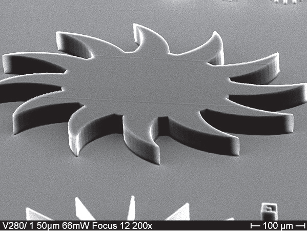
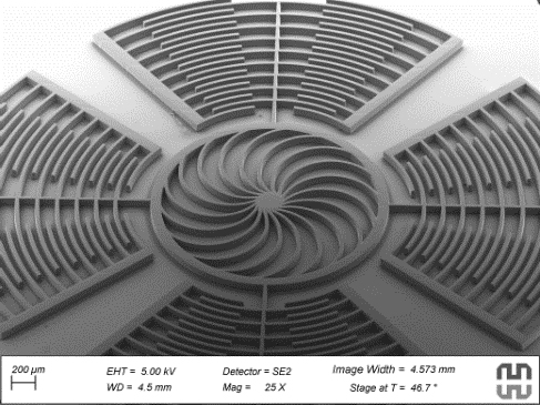
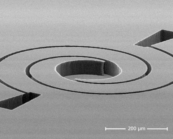
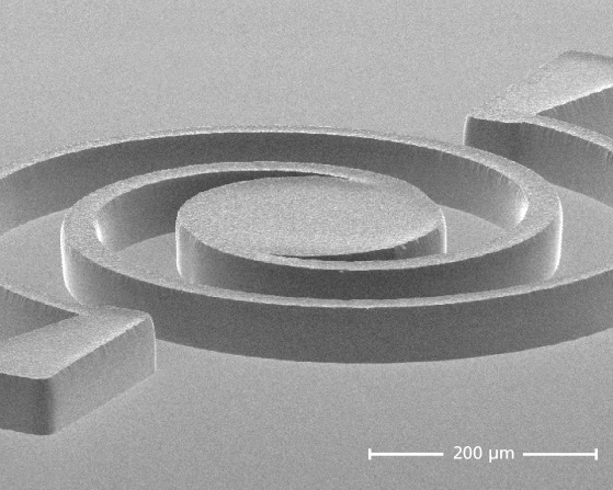
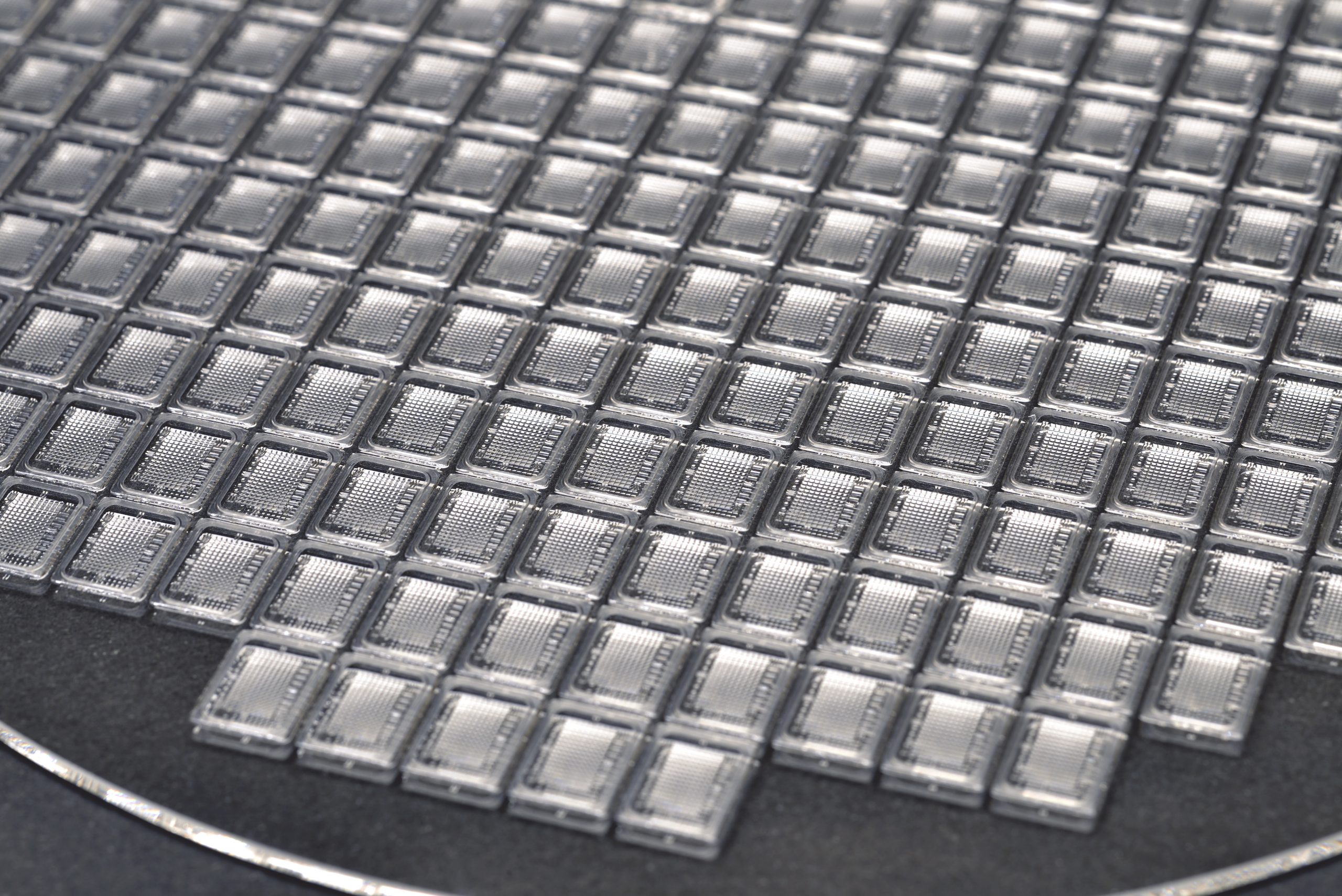
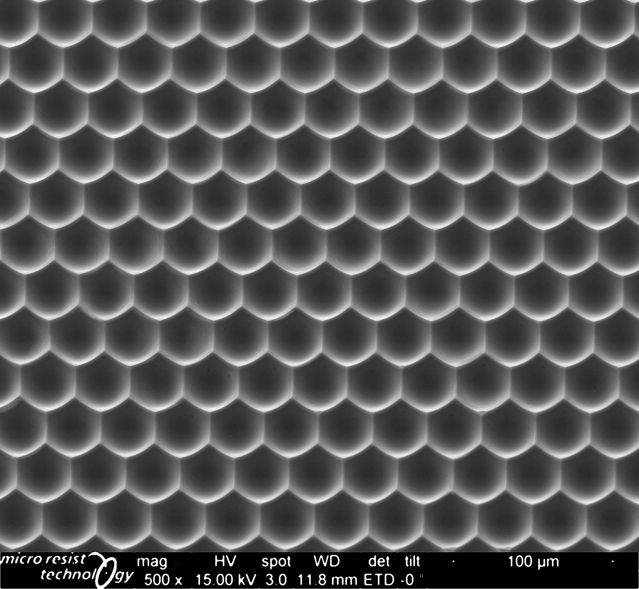
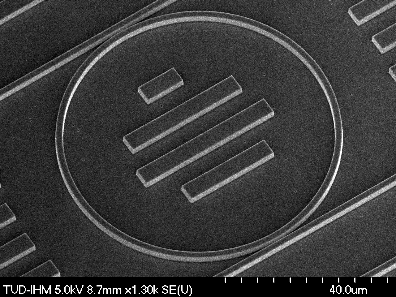
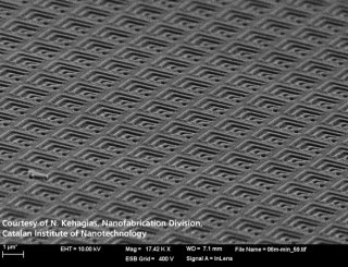
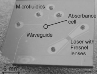
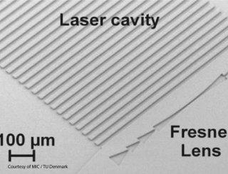
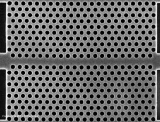
Step-and-repeat nanoimprint on pre-spin coated film for the fabrication of integrated optical devices
G Calafiore et al., J. Micro/Nanolith. MEMS MOEMS 14(3), 033506 Link to Abstract

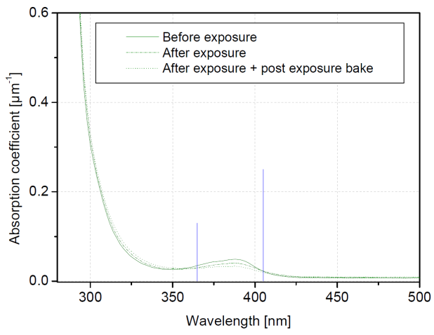
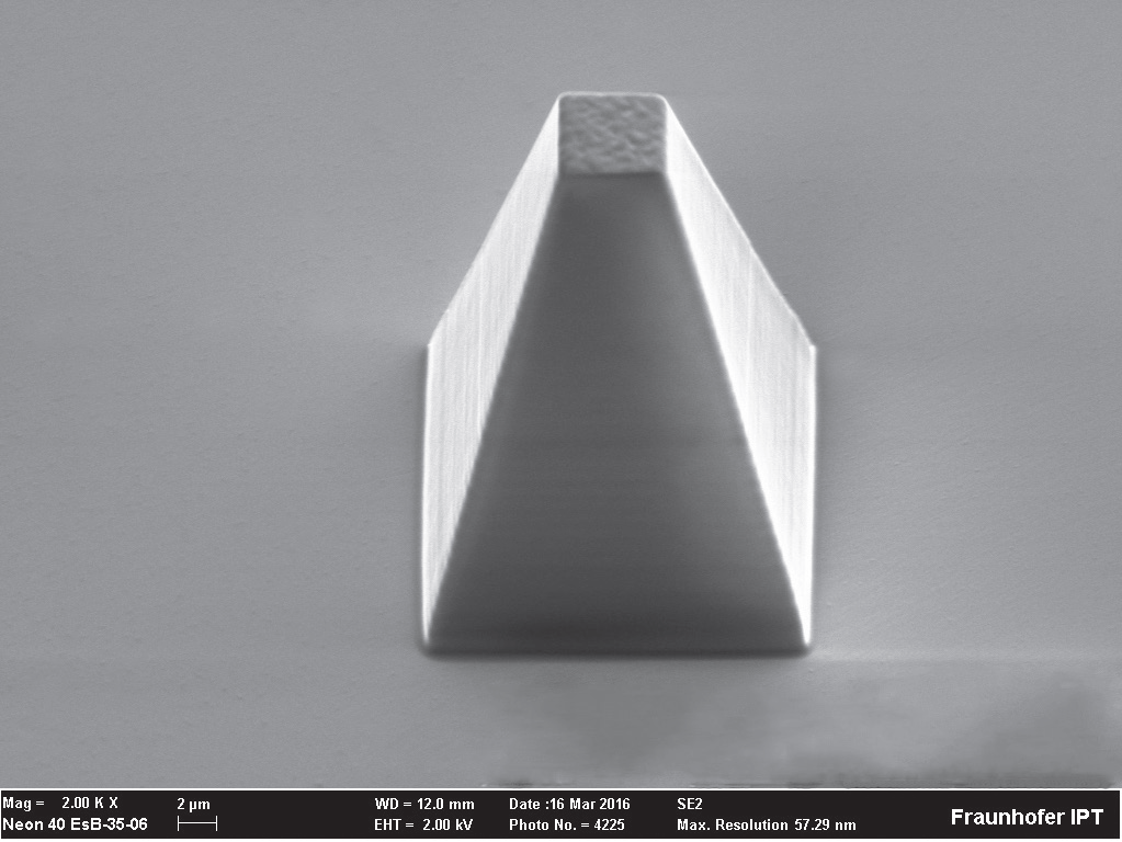
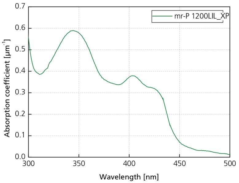
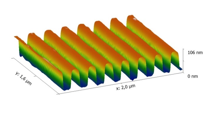
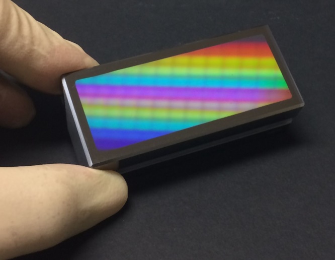
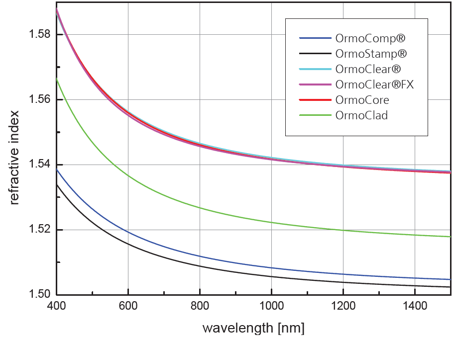
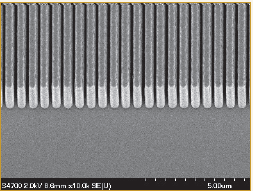
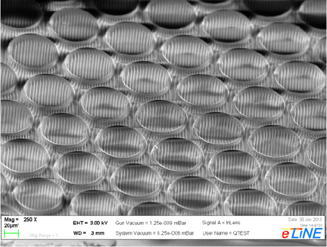
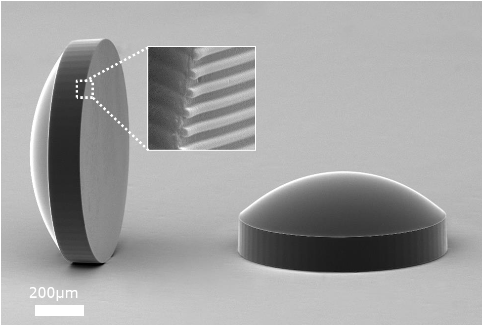
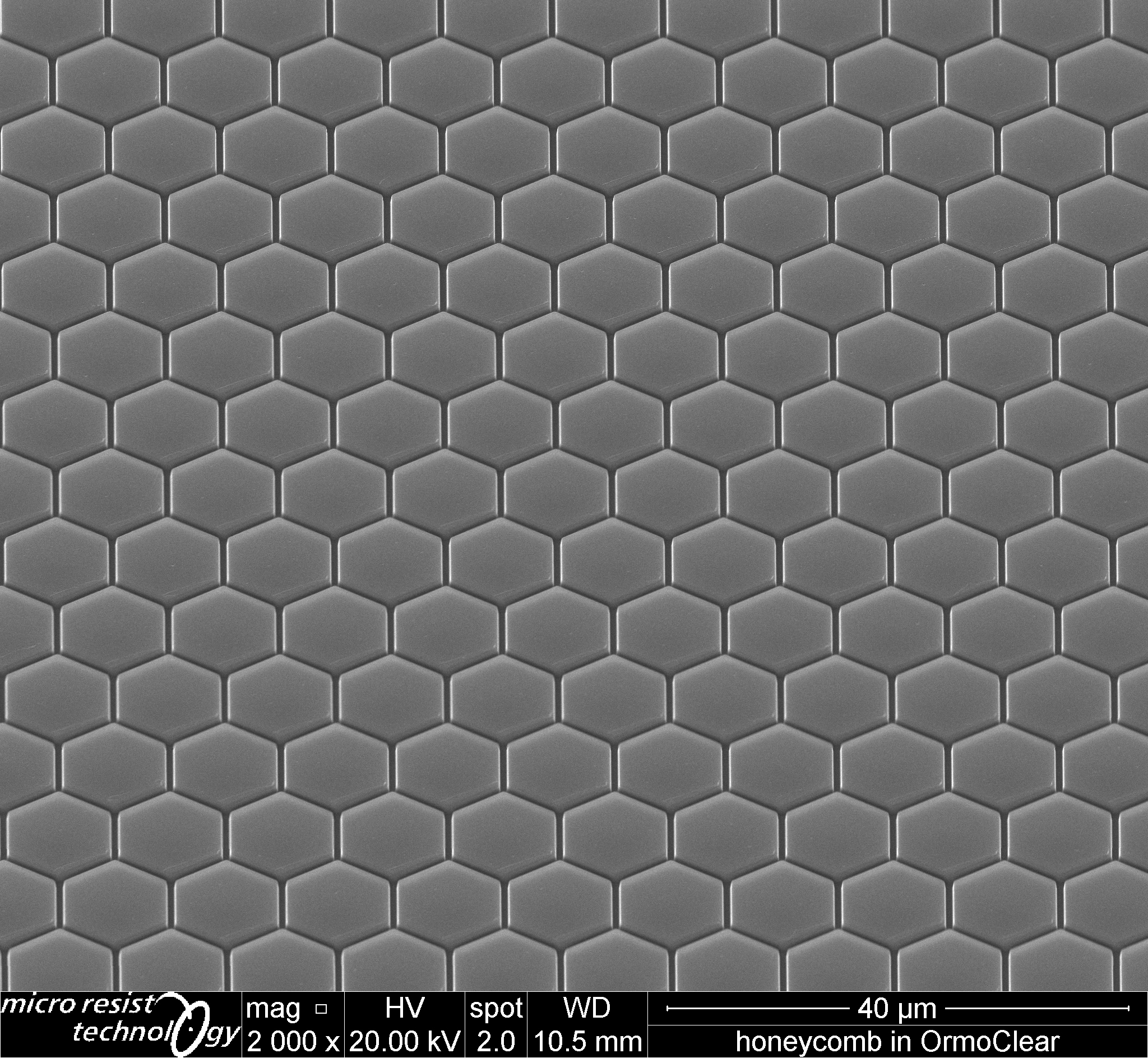
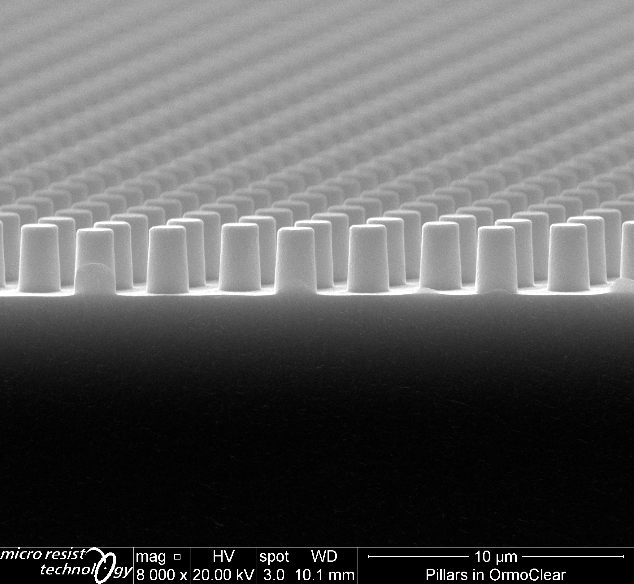
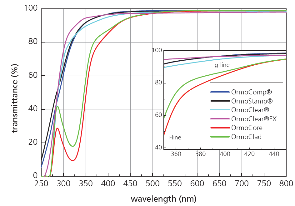
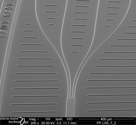
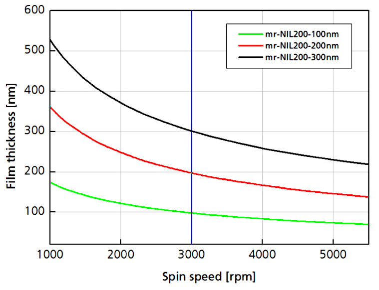
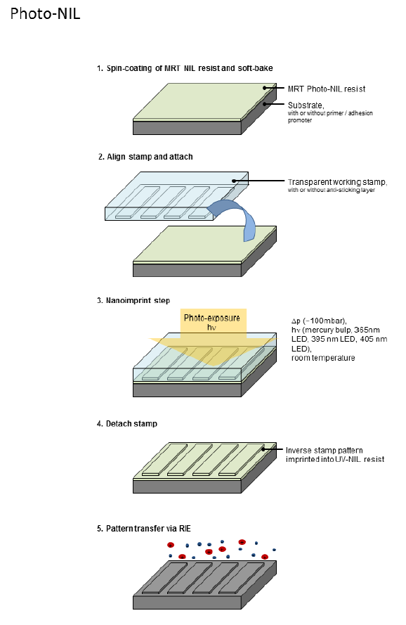
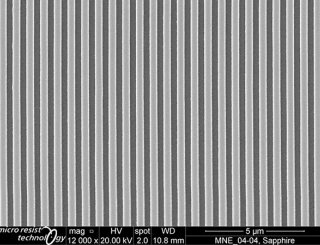
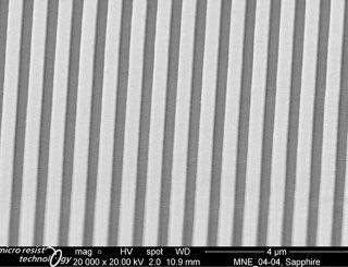
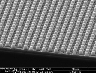
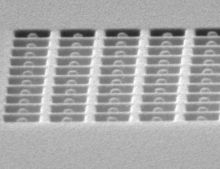
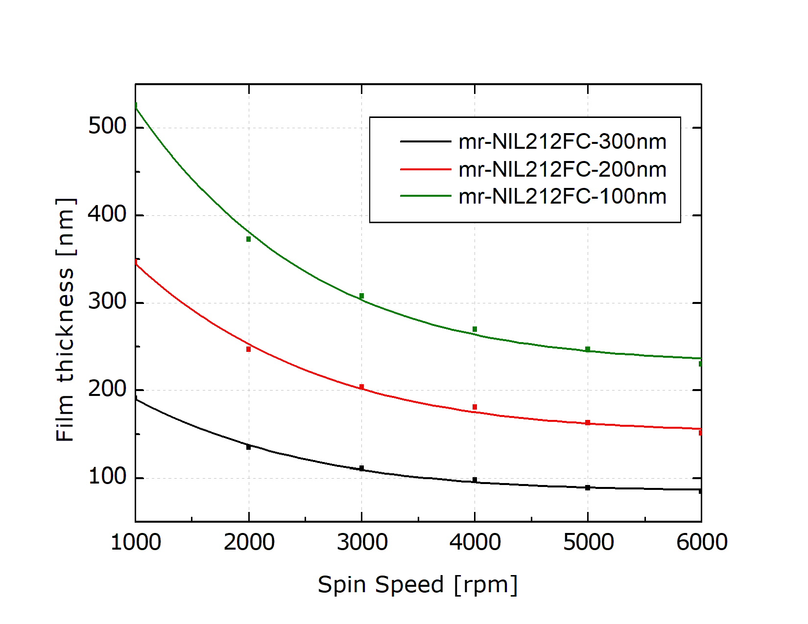
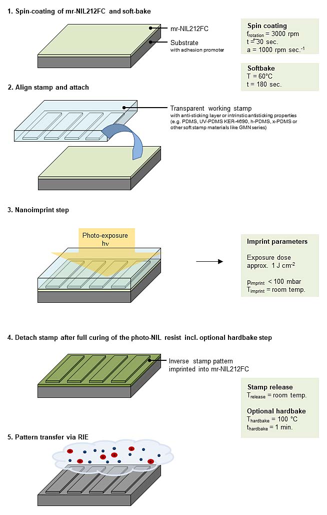
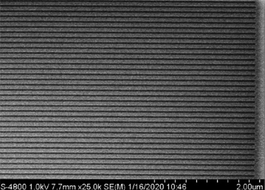
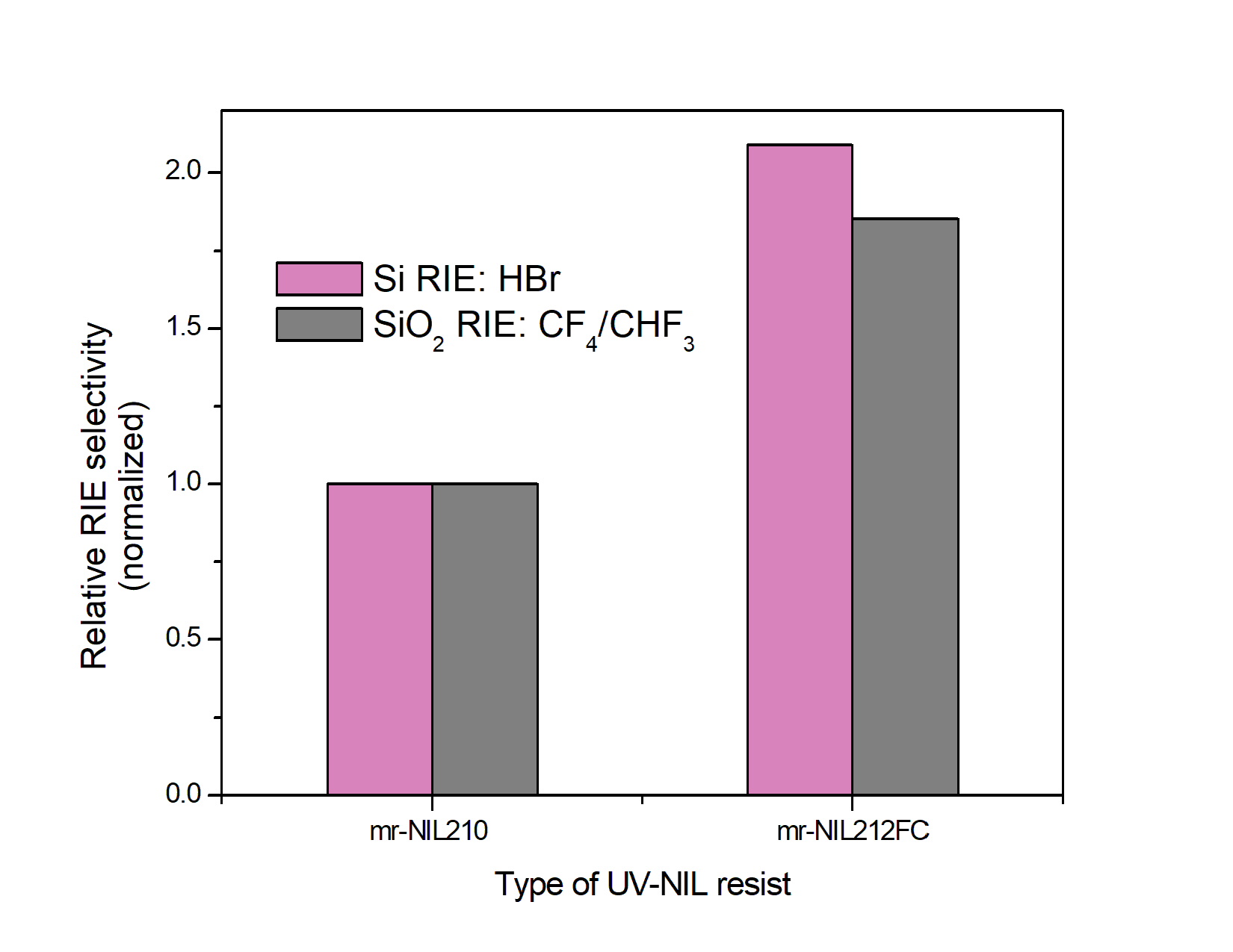
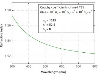
Efficient fabrication of photonic and optical patterns by imprinting the tailored photo-curable NIL resist «mr-NIL200»
M Messerschmidt et al., Poster, International Conference on Micro & Nano Engineering MNE2018, Copenhagen Link to Poster

UV-NIL

Resist Film Thickness [nm]
spin coating @ 3000 rpm
Recommended working stamp material Special Feature
mr-NIL200-100nm 100 non-porous No primer required, r.t. process
mr-NIL200-200nm 200
mr-NIL200-300nm 300

Film thickness and packages size

Specifications Film thickness and packages sizes
Ready to use solutions for standard film thickness (3000 rpm) mr-NIL200-100 nm
mr-NIL200-200 nm
mr-NIL200-300 nm
Customized film thickness upon request between (3000 rpm) 1 µm
Availalbe resist quantities 250 ml
500 ml
Larger volumes on request

Recommended process chemicals:

Thinner: mr-T 1078
Primer: Not needed
(mr-APS1 for mr-NIL200 film thickness > 300nm)
Omnicoat (Kayaku Advanced Materials)

quotation request

Clear
mr-NIL210 series
Nanoimprint Resists
Dry etch mask
Element 25weqwf
Photo-curable NIL-Resist
mr-NIL210 is a purely organic, photo-curable NIL resist with oustanding dry etch characteristics. It features an excellent curing and nanoimprint performance and is particularly suitable for soft-NIL using soft stamp materials, e.g. PDMS.
Unique Features
  • Excellent curing properties, even under air (presence of oxygen)
  • Compatibility to PDMS working stamps for soft-NIL, preferably applied in combination with UV-PDMS KER-4690 
  • Outstanding dry etch stability against various substrates like silicon, quartz, or aluminum
  • Purely organic resist, residue-free removable with oxygen plasma possible after curing
Applications
  • Etch mask for pattern transfer processes (dry and wet etching)
  • Fabrication of nanostructures for
    • LEDs, photonic crystals
    • Patterned sapphire substrates (PSS)
    • Microelectronics
    • Organic electronics (OLED, OPV, OTFT)
    • Data storage (bit patterned media)
    • Lift-off applications in combination with  e.g. LOR (MCC, USA)

UV-NIL

Resist Film Thickness [nm]
spin coating @ 3000 rpm
Recommended working stamp material Special Feature
mr-NIL210-100nm 100 porous soft stamp (e.g. PDMS) Excellent film stability, r.t. process
mr-NIL210-200nm 200
mr-NIL210-500nm 500

Our standard film thicknesses

mr-NIL210 Version Film thickness @3000 rpm*
mr-NIL210-100nm 100 nm
mr-NIL210-200nm 200 nm
mr-NIL210-500nm 500 nm

* Customized film thickness available on request up to 12.5 µm

Recommended process chemicals:

Thinner: mr-T 1078
Primer: mr-APS1, Omnicoat (Kayaku Advanced Materials)

quotation request

Clear
mr-NIL212FC series
Nanoimprint Resists
Dry etch mask
Element 25weqwf
Photo-curable NIL-Resist
mr-NIL212FC is a purely organic, photo-curable NIL resist with oustanding dry etch characteristics. It features an excellent curing and nanoimprint performance and is particularly suitable for soft-NIL using soft stamp materials, e.g. PDMS. mr-NIL212FC features a strongly increased etching stability in RIE processes compared to mr-NIL210.
Unique Features
  • Excellent structure stability due to the integrated FC-technology (fast curing) for sub-100nm-structures
  • Perfect curing characteristics in combination with low power light exposure sources (e.g. standard mask aligners)
  • Compatibility to PDMS working stamps for soft-NIL, preferably applied in combination with UV-PDMS KER-4690 
  • Provides superior etching selectivity compared to mr-NIL210 in RIE processes
  • Purely organic resist, residue-free removable with oxygen plasma possible after curing
  • Etch mask for pattern transfer processes (dry and wet etching)
  • Fabrication of nanostructures for
    • LEDs, photonic crystals
    • Patterned sapphire substrates (PSS)
    • Microelectronics
    • Organic electronics (OLED, OPV, OTFT)
    • Data storage (bit patterned media)
    • Lift-off applications in combination with  e.g. LOR (KAM, USA)

UV-NIL

Resist Film Thickness [nm]
spin coating @ 3000 rpm
Recommended working stamp material Special Feature
mr-NIL212FC-100nm 100 porous soft stamp (e.g. PDMS) Excellent film stability, r.t. process
mr-NIL212FC-200nm 200
mr-NIL212FC-300nm 300

Our standard film thicknesses

mr-NIL212FC version Film thickness @3000 rpm*
mr-NIL212FC-100nm 100 nm
mr-NIL212FC-200nm 200 nm
mr-NIL212FC-300nm 300 nm

* Customized film thickness available upon request

Recommended process chemicals:

Thinner: mr-T 1050

Primer: mr-APS1, OmniCoat (Kayaku Advanced Materials)

quotation request

Clear
mr-XNIL26SF
Nanoimprint Resists
Dry etch mask
Element 25weqwf
Photo-curable NIL resist, solvent-free
Photo-curable NIL resist featuring high content of fluorinated components
Unique Features
  • high content of fluorinated components for easy stamp release and low defectivity
  • 100% organic, easy strippable with oxygen plasma
  • Can be diluted to 100nm film thickness using PGMEA or ma-T 1050
  • Low refractive index of cured material (RI = 1.40)
Applications
  • NIL applications where comparably low release forces are essential (e.g. imprints on top of a multilayer stack)

UV-NIL

Resist Film Thickness [nm]
spin coating @ 3000 rpm
Recommended working stamp material Special Feature
mr-XNIL26SF 4.8 non-porous High fluorine content, low release forces, r.t. process, low RI, solvent-free

quotation request

Clear
mr-I T85 series
Nanoimprint Resists
Bio-Applications, Lab-on-Chip
Element 25weqwf
Non-polar thermoplastic NIL Resist
T-NIL resist (Tg = 85 °C) based on non-polar cyclo-olefin-copolymers (TOPAS)
Unique Features
  • Film thickness of up to 5 µm possible for the fabrication of microfluidic or lab-on-chip devices
  • 100% organic thermoplast → dry etching and stripping possible with pure oxygen plasma
  • featuring the highest optical transparency in the range of UV/vis and distinctive chemical stability against e.g. different solvents, acids, and bases
Applications

Lab-on-chip systems

  • Bio applications
  • Microfluidics
  • Microoptical elements
  • Wave guides
  • Single and multilayer systems
  • Mask for pattern transfer processes

T-NIL

Resist Film Thickness [nm]
spin coating @ 3000 rpm
GGlass transition temperature Tg [°C] Special Feature
mr-I T85-0.3 300 85 high chemical and optical stability, high transparency
mr-I T85-1.0 1000
mr-I T85-5.0 5000


Material characteristics and imprint parameters mr-I T85
Glass transition temperature Tg 85 °C
Imprint temperature 130 – 150 °C
PImprint pressure 5 – 20 bar
Ready-to-use solutions for various film thicknesses (3000 rpm) * mr-I T85-0.3 300 nm

mr-I T85-1.0 1.0 µm

mr-I T85-5.0 5.0 µm

Resist removal Oxygen plasma

* Customized film thickness up to 20 µm available on request

quotation request

Clear
mr-I 7000R series
Nanoimprint Resists
Dry etch mask
Element 25weqwf
Thermoplastic NIL resist
T-NIL resist featuring low glass transition temperature (Tg = 55 °C) for low temperature imprints
Unique Features
  • Facilitated stamp separation due to integrated fluorinated additive
  • 100% organic thermoplast → dry etching and stripping possible with pure oxygen plasma
  • Polymer soluble in aceton and other common solvents → easy cleaning
  • mr-I 7000R contains a fluorinated additive for lowering the release force during stamp detachment. The additive-free basic imprint polymer mr-I 7000E is available on request.
Applications

Fabrication of nanopatterns by pattern transfer for e.g

  • High brightness LEDs
  • Photonic crystals
  • Patterned media
  • Nano-optical devices, subwavelength optical elements
  • Microfluidics, bio applications
  • Single layer lift-off

T-NIL

Resist Film Thickness [nm]
spin coating @ 3000 rpm
Glass transition temperature Tg [°C] Special Feature
mr-I 7010R 100 55 Low Tg, high etching selectivity
mr-I 7020R 200
mr-I 7030R 300


Parameter mr-I 7000R mr-I 8000R
Glass transition temperature Tg 55 °C 115 °C
Imprint temperature 120 °C - 140 °C 150 °C - 180 °C
Imprint pressure 5 – 10 bar 20 - 40 bar
Ready-to-use solutions for standard film thicknesses *(3000 rpm) mr-I 7010R 100nm

mr-I 7020R 200nm

mr-I 7030R 300nm

mr-I 8010R 100nm

mr-I 8020R 200nm

mr-I 8030R 300nm

Resist thinner ma-T 1050 ma-T 1050
Resist stripping ma-T 1050, aceton, org. solvents or oxygen plasma ma-T 1050, aceton, org. solvents or oxygen plasma

* Customized film thickness up to 5 µm available on request

Recommended process chemicals:

Thinner: ma-T 1050
Remover: ma-T 1050, aceton, org. solvents or oxygen plasma

quotation request

Clear

If necessary, please also use the general contact on our website – we will get back to you as soon as possible!

Element 32
0

Negative Photoresists

Photoresists for UV (mask aligner, laser)/ DUV and e-beam lithography

  • Effective for broadband and i-line, Deep UV, e-beam exposure, or laser direct writing @ 405 nm
  • Lift-off resists with tunable pattern profile, high temperature stability up to 160 °C
  • Variety of viscosities for different film thicknesses in one spin-coating step
     
  • For pattern transfer: Physical vapour deposition (PVD) and single  layer lift-off, etch mask, mould for electroplating
  • For permanent applications: Polymeric waveguides
  • Use in microsystems technology, microelectronics, micro-optics  – manufacture of e.g. LEDs, ICs, MEMS, flat panel displays, fiber optics telecommunications devices

Positive Photoresists

Positive Photoresists for UV lithography (mask aligner, laser, greyscale exposure) and e-beam lithography

  • Variety of viscosities for 0.1 µm – 60 µm film thickness in one spin-coating step
  • Effective for broadband, g-line, h-line or i-line exposure, laser direct writing at 350…450 nm and e-beam lithography
  • No post exposure bake
  • Easy removal
     
  • For pattern transfer: Etch mask, mould for electroplating, mould for UV moulding
  • Use in microsystems technology, microelectronics, micro-optics – manufacture of e.g. MEMS, LEDs, ICs, MOEMS, fiber optics telecommunications devices, flat panel displays

Hybrid Polymers

micro resist technology offers a broad portfolio of UV-curable hybrid polymer products for micro-optical applications. Their excellent optical transparency and high thermal stability makes them perfectly suitable for the production of polymer-based optical components and waveguides. The main fields of application are micro lenses, diffractive optical elements (DOE), gratings, and single-mode or multi-mode waveguides.

OrmoComp®: DE 30 210 075 433; IR 1 091 982 ; TW 100030626; OrmoClear®: DE 30 210 075 434; IR 1 091 359 ; TW 100030628; OrmoStamp®: DE 30 210 075 435; IR 1 092 621 ; TW 100030629; OrmoPrime®: DE 30 210 075 436

Nanoimprint Resists

Nanoimprint Lithography (NIL) is a straight forward, low cost, and high throughput capable technology for the fabrication of nanometer scaled patterns. Main application fields are photonics, next generation electronics, as well as bio- and sensor applications.

micro resist technology GmbH has provided tailor-made resist formulations for nanoimprint lithography (NIL) since 1999. The unique key features of our products are outstanding film forming and imprinting performance beside excellent pattern fidelity and plasma etch stability. Besides our highly innovative material developments in close contact to industrial needs, our strength is the ability to adjust our materials in film thickness as well as addressing certain needs of the specific use cases within the formulation. Our nanoimprint resists are mostly applied as an etch mask for pattern transfer into various substrates, like Si, SiO2, Al or sapphire.

Our portfolio covers materials for the classical thermal NIL (T-NIL), in which a thermoplastic polymer is used, as well as UV-NIL, in which a liquid formulation is photo crosslinked upon photo exposure. With our technological expertise and know-how we are able to find the right material for your process and applications. Please contact us for your technical support!

Functional materials for inkjet-printing

Special designed functional materials from the product groups Hybrid Polymers, Photoresists, and Nanoimprint Polymers for the deposition and alternative patterning using inkjet printing process

  • Available in different viscosities (adjustable)
  • Suitable in commercial inkjet printing devices
  • Focused on high reliability of droplet generation
  • UV-curable formulations


  • Usable as a permanent material for optical application (e.g. lenses, wave guides, optical couplers, diffractive elements, …)
  • Packaging material in the micro electronic
  • Deposition / patterning on substrates with surface topography
  • Imprint material for nano-structuring with high dose accuracy

Dry Films

Dry films are ready-to-use polymer films as laminate foil with a high accuracy of the film thickness and excellent adhesion behaviour on various substrates. They are very simple in handling, photo-structurable and both as cut sheets and as roll material available.

  • Available in different film thicknesses
  • UV-crosslinking as negative photoresist
  • Feasibility of high aspect ratios
  • Vertical sidewalls
  • Multi lamination possible – up to 6 layer  complex multi-layer designs
  • High chemical resilience


  • Application as permanent material for optical application (e.g. lenses, wave guides …), in micro fluidics

Resist Alliance

micro resist technology is a single entry point for specialty chemicals used in micro and nano manufacturing in Europe. The portfolio of in-house products is complemented by the strategic sales of associated products that are manufactured by our international partners. Here we act as a high-service distributor and offer European medium-sized companies a wide range of complementary products from a single source, which can be used for both established and innovative production and manufacturing processes.

DuPont Electronic Solutions (formerly DOW Electronic Materials / Rohm and Haas Europe Trading ApS)

We offer products for semiconductor technologies, advanced packaging and dry film resists from our partner DuPont, with whom we have been working for more than 20 years.

Kayaku Advanced Materials, Inc. (formerly MicroChem Corp.)

We offer photoresists and specialty chemicals for MEMS and microelectronic applications from our partner Kayaku Advanced Materials, with whom we have been working for more than 20 years.

DJ MicroLaminates, Inc.

We offer dry film resists for MEMS, microfluidics and packaging applications from our partner DJ MicroLaminates, with whom we have been cooperating for over two years.