Element 2
+49 30 641 670 100
Element 1
info@microresist.de
Functional Materials for Inkjet-printing
30. Juni 2020

micro resist technology offers functional materials for Inkjet-printing. The materials have been specially designed to exhibit a good compatibility to a broad range of inkjet printing tools.

The portfolio involves two classes of products providing ideal solutions for the manufacture of micro and nano optical components or functional films. InkOrmo and InkEpo exhibit excellent optical properties as well as high chemical, mechanical and thermal stability. mr-UVCur26SF is solvent-free material which has been specifically designed for nanoimprint lithography (NIL).
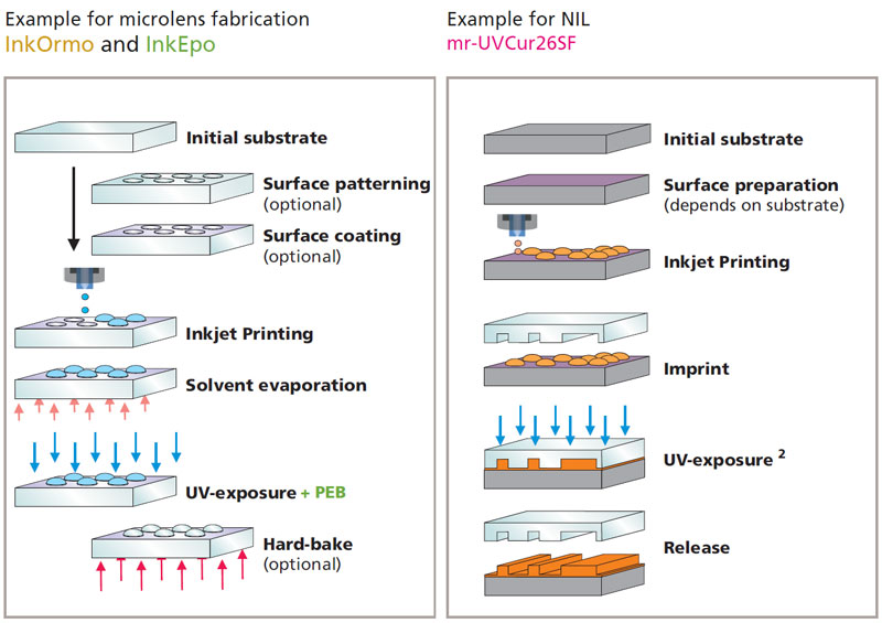
Process

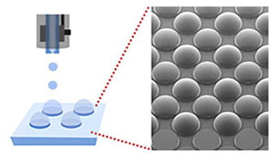
A) Microlenses by inkjet printing:

  • Typical lens size ranges from 50 µm to 1000 µm, but not exclusive
  • Lens aspect ratio (height/diameter) controlled by substrate pre-treatment
  • Lens profile with high level of freedom possible based on pre-patterned substrate
  • Lens size (diameter & height) controlled by printed volume / lens

B) Nanoimprint-lithography:

  • Step&Repeat process and continuous roll-to-roll (R2R ) UV-NIL processes
  • Large-area nanostructuring of flexible substrates
  • Ultra-high photocuring rate enabling high roller speeds and high throughput
  • R2R web speeds up to 30 m/min demonstrated

Special Features

  • Compatible with commercial inkjet printing devices
  • UV-curable materials
  • Solvent-containing and solvent-free inkjettable materials

Applications

  • Optical components (transparency)
  • Packaging (chemical inertness and optical and mechanical stability)
  • High volume manufacturing of antireflective coatings, (super)hydrophobic patterns on flexible substrates and wire-grid polarizers
  • Etch mask for plasma etching (excellent dry etch stability for pattern transfer)

micro resist technology GmbH provides customized solutions on request, e.g. for specific viscosities. Please contact us direct

Links to related product pages

Inkjet Materials
Inkjet-printing
3D microstructures
Nano and micro electronics
Wire-grid polarizers
Diffractive optical elements (DOE)
Organic electronics
InkOrmo series
InkEpo series
mr-UVCur26SF series
Share on email
Share on telegram
Share on whatsapp
Share on twitter
Share on facebook
Share on linkedin

Kontaktieren Sie uns.

Pflichtfelder sind mit einem * gekennzeichnet.
Element 32
0

Resist Alliance

micro resist technology is a single entry point for specialty chemicals used in micro and nano manufacturing in Europe. The portfolio of in-house products is complemented by the strategic sales of associated products that are manufactured by our international partners. Here we act as a high-service distributor and offer European medium-sized companies a wide range of complementary products from a single source, which can be used for both established and innovative production and manufacturing processes.

DuPont Electronic Solutions (formerly DOW Electronic Materials / Rohm and Haas Europe Trading ApS)

We offer products for semiconductor technologies, advanced packaging and dry film resists from our partner DuPont, with whom we have been working for more than 20 years.

Kayaku Advanced Materials, Inc. (formerly MicroChem Corp.)

We offer photoresists and specialty chemicals for MEMS and microelectronic applications from our partner Kayaku Advanced Materials, with whom we have been working for more than 20 years.

DJ MicroLaminates, Inc.

We offer dry film resists for MEMS, microfluidics and packaging applications from our partner DJ MicroLaminates, with whom we have been cooperating for over two years.

Dry Films

Dry films are ready-to-use polymer films as laminate foil with a high accuracy of the film thickness and excellent adhesion behaviour on various substrates. They are very simple in handling, photo-structurable and both as cut sheets and as roll material available.

  • Available in different film thicknesses
  • UV-crosslinking as negative photoresist
  • Feasibility of high aspect ratios
  • Vertical sidewalls
  • Multi lamination possible – up to 6 layer  complex multi-layer designs
  • High chemical resilience


  • Application as permanent material for optical application (e.g. lenses, wave guides …), in micro fluidics

Functional materials for inkjet-printing

Special designed functional materials from the product groups Hybrid Polymers, Photoresists, and Nanoimprint Polymers for the deposition and alternative patterning using inkjet printing process

  • Available in different viscosities (adjustable)
  • Suitable in commercial inkjet printing devices
  • Focused on high reliability of droplet generation
  • UV-curable formulations


  • Usable as a permanent material for optical application (e.g. lenses, wave guides, optical couplers, diffractive elements, …)
  • Packaging material in the micro electronic
  • Deposition / patterning on substrates with surface topography
  • Imprint material for nano-structuring with high dose accuracy

Nanoimprint Resists

Nanoimprint Lithography (NIL) is a straight forward, low cost, and high throughput capable technology for the fabrication of nanometer scaled patterns. Main application fields are photonics, next generation electronics, as well as bio- and sensor applications.

micro resist technology GmbH has provided tailor-made resist formulations for nanoimprint lithography (NIL) since 1999. The unique key features of our products are outstanding film forming and imprinting performance beside excellent pattern fidelity and plasma etch stability. Besides our highly innovative material developments in close contact to industrial needs, our strength is the ability to adjust our materials in film thickness as well as addressing certain needs of the specific use cases within the formulation. Our nanoimprint resists are mostly applied as an etch mask for pattern transfer into various substrates, like Si, SiO2, Al or sapphire.

Our portfolio covers materials for the classical thermal NIL (T-NIL), in which a thermoplastic polymer is used, as well as UV-NIL, in which a liquid formulation is photo crosslinked upon photo exposure. With our technological expertise and know-how we are able to find the right material for your process and applications. Please contact us for your technical support!

Hybrid Polymers

micro resist technology offers a broad portfolio of UV-curable hybrid polymer products for micro-optical applications. Their excellent optical transparency and high thermal stability makes them perfectly suitable for the production of polymer-based optical components and waveguides. The main fields of application are micro lenses, diffractive optical elements (DOE), gratings, and single-mode or multi-mode waveguides.

OrmoComp®: DE 30 210 075 433; IR 1 091 982 ; TW 100030626; OrmoClear®: DE 30 210 075 434; IR 1 091 359 ; TW 100030628; OrmoStamp®: DE 30 210 075 435; IR 1 092 621 ; TW 100030629; OrmoPrime®: DE 30 210 075 436

Positive Photoresists

Positive Photoresists for UV lithography (mask aligner, laser, greyscale exposure) and e-beam lithography

  • Variety of viscosities for 0.1 µm – 60 µm film thickness in one spin-coating step
  • Effective for broadband, g-line, h-line or i-line exposure, laser direct writing at 350…450 nm and e-beam lithography
  • No post exposure bake
  • Easy removal
     
  • For pattern transfer: Etch mask, mould for electroplating, mould for UV moulding
  • Use in microsystems technology, microelectronics, micro-optics – manufacture of e.g. MEMS, LEDs, ICs, MOEMS, fiber optics telecommunications devices, flat panel displays

Negative Photoresists

Photoresists for UV (mask aligner, laser)/ DUV and e-beam lithography

  • Effective for broadband and i-line, Deep UV, e-beam exposure, or laser direct writing @ 405 nm
  • Lift-off resists with tunable pattern profile, high temperature stability up to 160 °C
  • Variety of viscosities for different film thicknesses in one spin-coating step
     
  • For pattern transfer: Physical vapour deposition (PVD) and single  layer lift-off, etch mask, mould for electroplating
  • For permanent applications: Polymeric waveguides
  • Use in microsystems technology, microelectronics, micro-optics  – manufacture of e.g. LEDs, ICs, MEMS, flat panel displays, fiber optics telecommunications devices