Process parameters for inkjet dispensing
| Process step | Process parameter |
| Inkjet parameter | Piezo actuated printhead, dispensing possible at room temperature |
| Prebake | Not necessary (solvent-free) |
| Imprint temperature | Room temperature |
| Imprint pressure | > 100 mbar |
| Radiation dose | > 500 mJ cm-2 (λ = 320 – 420 nm) |
| Thinner | Not recommended |
| Primer | mr-APS1 (e.g. for Si) |
Process parameters for roll-to-roll NIL
| Process step | Process parameter |
| Resist application method | Gravure printing, inkjet dispensing, etc. |
| Prebake | Not necessary (solvent-free) |
| Web speed | Depending on and limited by tool setup and light source, up to 30 m/min shown so far |
| Imprint temperature | Room temperature |
| Imprint pressure | Depending on roller imprinter |
| Radiation dose | > 500 mJ cm-2 (λ = 320 – 420 nm) |
| Thinner | Not recommended |
| Primer | Not necessary (good adhesion to PC, PET, etc.) |
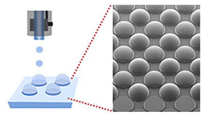
Inkjetable and photo-curable resists for large-area and high-throughput roll-to-roll nanoimprint lithography
M W Thesen et al., Journal of micro/nanolithography, MEMS and MOEMS 13 (2014), Nr.4, Art. 043003
Link: DOI: 10.1117/1.JMM.13.4.043003
Fabrication of Large-Area Flexible SERS Substrates by Nanoimprint Lithography
V Suresh et al., ACS Appl. Nano Mater. 2018, 1, 2, 886-893
Link: https://pubs.acs.org/doi/abs/10.1021/acsanm.7b00295
micro resist technology is a single entry point for specialty chemicals used in micro and nano manufacturing in Europe. The portfolio of in-house products is complemented by the strategic sales of associated products that are manufactured by our international partners. Here we act as a high-service distributor and offer European medium-sized companies a wide range of complementary products from a single source, which can be used for both established and innovative production and manufacturing processes.
DuPont Electronic Solutions (formerly DOW Electronic Materials / Rohm and Haas Europe Trading ApS)
We offer products for semiconductor technologies, advanced packaging and dry film resists from our partner DuPont, with whom we have been working for more than 20 years.
Kayaku Advanced Materials, Inc. (formerly MicroChem Corp.)
We offer photoresists and specialty chemicals for MEMS and microelectronic applications from our partner Kayaku Advanced Materials, with whom we have been working for more than 20 years.
DJ MicroLaminates, Inc.
We offer dry film resists for MEMS, microfluidics and packaging applications from our partner DJ MicroLaminates, with whom we have been cooperating for over two years.
Dry films are ready-to-use polymer films as laminate foil with a high accuracy of the film thickness and excellent adhesion behaviour on various substrates. They are very simple in handling, photo-structurable and both as cut sheets and as roll material available.
Special designed functional materials from the product groups Hybrid Polymers, Photoresists, and Nanoimprint Polymers for the deposition and alternative patterning using inkjet printing process
Nanoimprint Lithography (NIL) is a straight forward, low cost, and high throughput capable technology for the fabrication of nanometer scaled patterns. Main application fields are photonics, next generation electronics, as well as bio- and sensor applications.
micro resist technology GmbH has provided tailor-made resist formulations for nanoimprint lithography (NIL) since 1999. The unique key features of our products are outstanding film forming and imprinting performance beside excellent pattern fidelity and plasma etch stability. Besides our highly innovative material developments in close contact to industrial needs, our strength is the ability to adjust our materials in film thickness as well as addressing certain needs of the specific use cases within the formulation. Our nanoimprint resists are mostly applied as an etch mask for pattern transfer into various substrates, like Si, SiO2, Al or sapphire.
Our portfolio covers materials for the classical thermal NIL (T-NIL), in which a thermoplastic polymer is used, as well as UV-NIL, in which a liquid formulation is photo crosslinked upon photo exposure. With our technological expertise and know-how we are able to find the right material for your process and applications. Please contact us for your technical support!
micro resist technology offers a broad portfolio of UV-curable hybrid polymer products for micro-optical applications. Their excellent optical transparency and high thermal stability makes them perfectly suitable for the production of polymer-based optical components and waveguides. The main fields of application are micro lenses, diffractive optical elements (DOE), gratings, and single-mode or multi-mode waveguides.
OrmoComp®: DE 30 210 075 433; IR 1 091 982 ; TW 100030626; OrmoClear®: DE 30 210 075 434; IR 1 091 359 ; TW 100030628; OrmoStamp®: DE 30 210 075 435; IR 1 092 621 ; TW 100030629; OrmoPrime®: DE 30 210 075 436
Positive Photoresists for UV lithography (mask aligner, laser, greyscale exposure) and e-beam lithography
Photoresists for UV (mask aligner, laser)/ DUV and e-beam lithography