Element 2
+49 30 641 670 100
Element 1
info@microresist.de
ma-N 1400 series
Negative Photoresists
PVD & Lift-off
Element 25weqwf
ma-N 1400 - Negative Tone Photoresist Series
for Conventional Pattern Transfer and Single-Layer Lift-Off Processes
Unique Features
  • Resists available in a variety of viscosities
  • Aqueous alkaline development
  • Tunable pattern profile: vertical to undercut
  • High wet and dry etch resistance
  • Good thermal stability of the resist pattern
  • Easy to remove
Applications
  • Microelectronics and micro systems technology
  • Mask for lift-off processes
  • Etch mask for semiconductors and metals
  • Well suitable for implantation
  • Mould for electroplating
Resist Film Thickness [µm]
spin coating @ 3000 rpm
Spectral Sensitivity Special Feature
ma-N 1405 0.5 300 - 410nm

i-line - 365 nm

(h-line - 405 nm)

Novolak based resist, thermal stability up to 160°C
for metal evaporation and sputtering
ma-N 1407 0.7
ma-N 1410 1.0
ma-N 1420 2.0
ma-N 1440 4.0
ma-N 402 0.2 300 - 380nm

i-line - 365 nm

Novolak based resist,
thermal stability up to 110°C
for metal evaporation
ma-N 405 0.5
ma-N 415 1.5
ma-N 420 2.0
ma-N 440 4.1
ma-N 490 7.5

Recommended process chemicals:

for ma-N 1400 Series
Thinner: ma-T 1046
Developer: ma-D 533/S (TMAH based)
Remover: mr-Rem 700 (NMP & NEP free), mr-Rem 500 (NMP free), ma-R 404/S (strongly alkaline)
Lift-off: mr-Rem 700 (NMP & NEP free), mr-Rem 500 (NMP free)

for ma-N 400 Series
Thinner: ma-T 1049
Developer: ma-D 331/S, ma-D 332/S (NaOH based), 531/S, ma-D 532/S (TMAH based)
Remover: mr-Rem 700 (NMP & NEP free), mr-Rem 500 (NMP free), ma-R 404/S (strongly alkaline)
Lift-off: mr-Rem 700 (NMP & NEP free), mr-Rem 500 (NMP free) 

quotation request

Clear
ma-N 400 series
Negative Photoresists
PVD & Lift-off
Element 25weqwf
ma-N 400 - Negative Tone Photoresist Series
for Conventional Pattern Transfer and Single-Layer Lift-Off Processes
Unique Features
  • Resists available in a variety of viscosities
  • Aqueous alkaline development
  • Tunable pattern profile: vertical to undercut
  • High wet and dry etch resistance
  • Good thermal stability of the resist pattern
  • Easy to remove
Application
  • Microelectronics and micro systems technology
  • Mask for lift-off processes
  • Etch mask for semiconductors and metals
  • Well suitable for implantation
  • Mould for electroplating
Resist Film Thickness [µm]
spin coating @ 3000 rpm
Spectral Sensitivity Special Feature
ma-N 402 0.2 300 - 380nm

i-line - 365 nm

Novolak based resist, thermal stability up to 110°C for metal evaporation
ma-N 405 0.5
ma-N 415 1.5
ma-N 420 2.0
ma-N 440 4.1
ma-N 490 7.5
ma-N 1405 0.5 300 - 410nm

i-line - 365 nm

(h-line - 405 nm)

Novolak based resist, thermal stability up to 160°C for metal evaporation and sputtering
ma-N 1407 0.7
ma-N 1410 1.0
ma-N 1420 2.0
ma-N 1440 4.0

Recommended process chemicals:

for ma-N 400 Series
Thinner: ma-T 1049
Developer: ma-D 331/S, ma-D 332/S (NaOH based), 531/S, ma-D 532/S (TMAH based)
Remover: mr-Rem 700 (NMP & NEP free), mr-Rem 500 (NMP free), ma-R 404/S (strongly alkaline)
Lift-off: mr-Rem 700 (NMP & NEP free), mr-Rem 500 (NMP free)

for ma-N 1400 Series
Thinner: ma-T 1046
Developer: ma-D 533/S (TMAH based)
Remover: mr-Rem 700 (NMP & NEP free), mr-Rem 500 (NMP free), ma-R 404/S (strongly alkaline)
Lift-off: mr-Rem 700 (NMP & NEP free), mr-Rem 500 (NMP free)

quotation request

Clear
ma-N 2400 series
Negative Photoresists
Dry etch mask
Element 25weqwf
ma-N 2400 - Negative Tone Photoresist Series
E-Beam and Deep UV sensitive
Unique Features ma-N 2400 series for e-beam and deep UV lithography
  • Resists available in a variety of viscosities
  • Aqueous alkaline development
  • Excellent pattern resolution - down to 30 nm
  • High wet and dry etch resistance
  • Good thermal stability
  • Easy to remove
Applications
  • Manufacturing of semiconductor devices
  • Use in micro- and nanoelectronics
  • Mask for etching, e.g. Si, SiO2, Si3N4 or metals
  • Mask for ion implantation
  • Stamp fabrication for NIL
Resist Film Thickness [µm] Spin Coating @ 3000 rpm Sensitivity Special Feature
ma-N 2401 0.1 E-beam

Deep UV: 248nm / 254nm

novolak based resist,

high wet and dry etch resistance

ma-N 2403 0.3
ma-N 2405 0.5
ma-N 2410 1.0

Recommended process chemicals:

Thinner: ma-T 1090
Developer: ma-D 525 (TMAH based), ma-D 331, ma-D 332 (NaOH based)
Remover: mr-Rem 700 (NMP & NEP free), mr-Rem 500 (NMP free), ma-R 404/S (strongly alkaline)

quotation request

Clear
mr-DWL series
Negative Photoresists
Mastering / micro-optics
Element 25weqwf
mr-DWL - Negative Tone Photoresist Series
For Direct Laser Writing (DLW) @ 405 nm & Two Photon Polymerization (2PP)
Unique Features
  • Specifically designed for exposure wavelengths above 400 nm
  • Suitable for DLW (e.g. @ 405 nm) & 2PP
  • High sensitivity
  • Excellent thermal and chemical stability
  • High wet and dry etch stability
Applications
  • Fast and contactless prototyping by DLW & 2PP
  • Etch mask for wet and dry etch processes
  • Mould for electroplating
  • Mould for stamp fabrication by thermal or UV moulding
  • Optical applications in micro systems technology
Resist Thickness range [µm]
Spin Coating @ 1000 - 6000 rpm
Spectral Sensitivity Special Feature
mr-DWL 5 3 - 15 350 nm - 410 nm

i-line/ h-line

designed for patterning by direct laser writing (DLW & 2PP),

high dry and wet etch resistance for non & permanent optical application

mr-DWL 40 10 - 100
mr-DWL 100 20 - 150

Recommended process chemicals:

Thinner: no thinner available
Developer: mr-Dev 600 (solvent based)
Remover: mr-Rem 700 (NMP & NEP free), mr-Rem 500 (NMP free), O2-Plasma

quotation request

Clear
EpoCore & EpoClad series
Negative Photoresists
Waveguides
Element 25weqwf
EpoCore & EpoClad - Negative Tone Photoresist Series
For manufacture of optical single mode (SM) & multi mode (MM) polymer waveguides
Unique Features
  • Standard UV lithography & PCB technology processing
  • UV patterning of core and cladding
  • High transmittance @ 850 nm
  • High heat (> 230 °C) and pressure resistance
  • Tunable refractive index (core/ cladding)
Applications
  • Optical SM & MM polymer waveguides
  • Biosensors (multifunctional systems)
  • Microfluidics
Resist Thickness range [µm]
spin coating @ 3000 rpm
Spectral Sensitivity Special Feature of manufactured waveguide
EpoCore 2 2 i-line - 365nm Refractive index @ 830 nm: EpoCore: 1.58, EpoClad: 1.57,
low shrinkage,
high thermal stability up to 230°C,
low optical loss ̴0.2dB/cm @ 850nm
EpoCore 5 5
EpoCore 10 10
EpoCore 20 20
EpoCore 50 50 (@ 1.500 rpm)
EpoClad 2 2
EpoClad 5 5
EpoClad 10 10
EpoClad 20 20
EpoClad 50 50 (@ 1.700 rpm)

Recommended process chemicals:

Thinner: no thinner available
Developer: mr-Dev 600 (solvent based)
Remover: mr-Rem 700 (NMP & NEP free), mr-Rem 500 (NMP free), O2-plasma

quotation request

Clear
mr-EBL 6000 series
Negative Photoresists
Dry etch mask
Element 25weqwf
mr-EBL 6000 - Negative Tone Resist Series
High E-beam sensitivity
Unique features
  • E-beam sensitivity:
    • 2 - 5 μC/cm2 @ 10 keV
    • 4 - 6 μC/cm2 @ 20 keV
    • 20 - 40 μC/cm2 @ 50 keV
  • Post exposure bake (PEB) necessary
  • Development in organic solvents
  • Excellent thermal stability of the resist patterns
  • High wet and dry etch resistance
  • Resolution capability: 80 nm
  • Use in micro- and nanoelectronics
  • Manufacturing of semiconductor devices
  • Mask for etching, e.g. of Si, SiO2, Si3N4 or metals
  • Generation of stamps with nanopatterns
Resist Film Thickness [µm]
Spin Coating @ 3000 rpm
Sensitivity Special Feature
mr-EBL 6000.1 0.1 E-beam excellent thermal stability,
high wet and dry etch resistance
mr-EBL 6000.3 0.3
mr-EBL 6000.5 0.5

Recommended process chemicals:

Thinner: ma-T 1045
Developer: mr-Dev 600 (solvent based)
Remover: mr-Rem 700 (NMP & NEP free), mr-Rem 500 (NMP free), O2-Plasma

quotation request

Clear
InkEpo series
Negative Photoresists
Inkjet Materials
Element 25weqwf
InkEpo series - UV curable material for inkjet-printing
Unique Features
  • UV-curable, solvent based inks
  • Low viscosities
  • Compatible to standard inkjet-printing devices
  • Excellent thermal, mechanical and chemical stability of cured patterns
  • High transparency to near UV and visible light
Applications
  • Single micro-lenses and micro-lens arrays
  • Waveguides and microfluidic devices
  • Spacers and protecting layers
  • Glue for bonding applications
  • Large-area substrate processing
Material Viscosity

[mPas]

Oxygen insensitive curing Refractive index (589 nm) after curing Temperature stability after curing Suggested applications
InkEpo series 5 ± 0.3

8 ± 0.5

12 ± 1

25 ± 1

No 1.555 Up to 180 °C Permanent optical applications (e.g. microlenses, waveguides)
Alternative Inkjet Materialien:
InkOrmo series 7 ± 1

12 ± 1.5

18 ± 2

No 1.517 – 1.520 Up to 270 °C Permanent optical applications (e.g. microlenses)
mr-UVCur26SF 15 ± 2

(lösungsmittelfrei)

Yes 1.518 Up to 180 °C Etch mask, Step & Repeat NIL processes, large-area structuring of flexible substrates

Recommended process chemicals:

Thinner: no thinner available
Developer: not required
Remover: mr-Rem 700 (NMP & NEP free), mr-Rem 500 (NMP free), O2-plasma

quotation request

Clear
MICROPOSIT ™ SPR350 ™ series
Positive Photoresists
Element 25weqwf
Positive Resist, g- and i-line multi wavelength exposure

quotation request

Clear
MICROPOSIT™ LOL™2000 Lift Off Layer
Element 25weqwf
Bi-Layer Lift-Off Processes
For Bi-Layer Lift-Off Processes

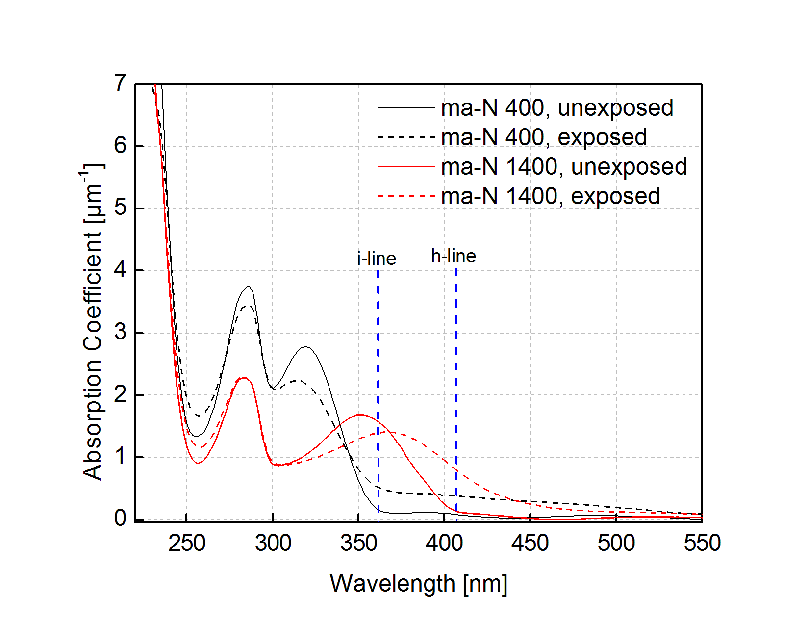
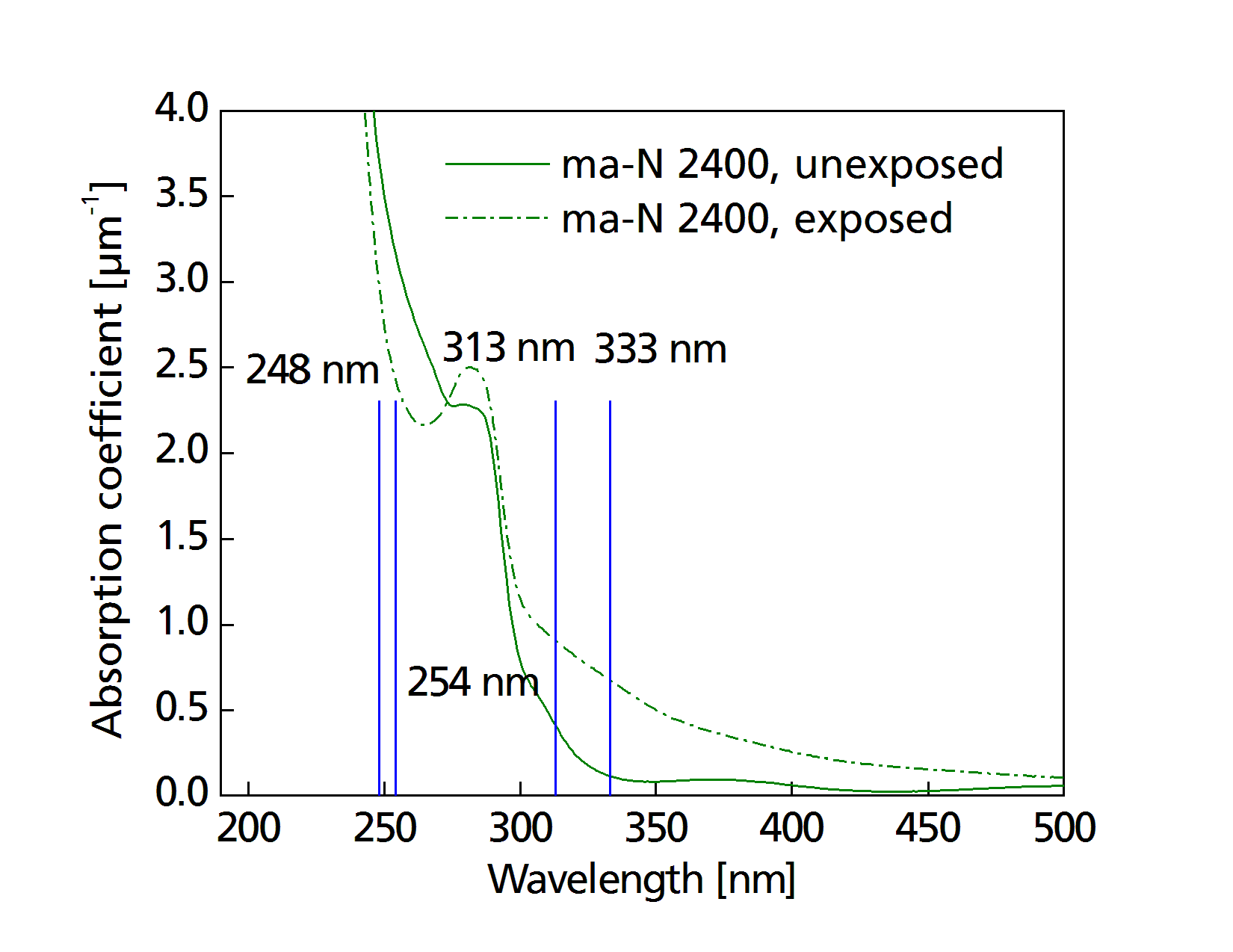
Microposit LOL 2000 lift-off layer is an enhanced dissolution rate, dyed PMGI (polyme- thylglutarimide) solution used for lift-off processes requiring tight CD control, such as GMR thinfilm head, GaAs, and other leading-edge semiconductor applications. The LOL bilayer lift-off process is suitable for applications where a thin layer of metal is sputtered or evaporated in an addi- tive process. CD variation due to etch bias inherent in substractive processes is eliminated, resulting in superiormetallinewidthcontrol.Attackonthe substrates by an etchant is eliminated.

Microposit FSC Series Surface Coating is available in two thickness ranges.
  • FSC-M: 2.4 to 3.3 μm
    For front-side protection during backlapping 0.2 μm filtration

quotation request

Clear
Microposit ™ FSC ™
Element 25weqwf
Protective Surface Coating

quotation request

Clear
UV ™ 60 series
Positive Photoresists
Element 25weqwf
Positive Resist, DUV

quotation request

Clear
UV ™ 1100 series
Positive Photoresists
Element 25weqwf
Positive Resist, DUV

quotation request

Clear
UV ™ 135G series
Positive Photoresists
Element 25weqwf
Positive Resist, DUV

quotation request

Clear
UVN ™ 2300 series
Negative Photoresists
Element 25weqwf
Negative Resist, DUV

quotation request

Clear
XR-1541 E-Beam Resist
Negative Photoresists
Element 25weqwf
Negative Tone HSQ E-Beam Resist

quotation request

Clear
SU-8 series
Negative Photoresists
Element 25weqwf
Thick Negative Epoxy Photoresists
Permanent Applications, High aspect ratio, photo-definable ultra-thick structures, Wide range of viscosities – 10-200 µm optimum thickness range
MATERIAL ATTRIBUTES
  • i-line imaging
  • High aspect ratio with vertical sidewalls
  • Photo-definable ultra-thick structures
  • Wide range of viscosities – 10-200 um optimum thickness range
  • Outstanding chemical and thermal stability
  • Excellent dry-etch resistance
  • Film thickness from 2 -> 200 µm with single spin coat processes
APPLICATIONS
  • MEMS
  • PDMS molding
  • Microfluidics
  • Inkjet nozzles

quotation request

Clear
SU-8 2000 series
Negative Photoresists
Element 25weqwf
Thick Negative Epoxy Photoresists
Permanent Applications
MATERIAL ATTRIBUTES
  • i-line imaging
  • High aspect ratio with vertical sidewalls
  • 0.5 -> 200 µm film thickness in a single coat
  • Improved substrate wetting
  • Faster drying and higher process throughput
  • Wide range of viscosities – 10-100 um optimum thickness range
  • Outstanding chemical and thermal stability
APPLICATIONS
  • MEMS
  • PDMS molding
  • Displays
  • Rapid prototyping

quotation request

Clear
SU-8 3000 series
Negative Photoresists
Element 25weqwf
Thick Negative Epoxy Photoresists
Permanent Applications
MATERIAL ATTRIBUTES
  • i-line imaging
  • High aspect ratio with vertical sidewalls
  • Up to 100 µm film thickness in a single coat
  • Improved substrate adhesion
  • Reduced coating stress
  • Wide range of viscosities – 10-70 um optimum thickness range
  • Outstanding chemical and thermal stability
APPLICATIONS
  • MEMS
  • PDMS molding
  • Waveguides
  • Microfluidics

quotation request

Clear
SU-8 TF 6000 series
Negative Photoresists
Element 25weqwf
High Resolution Thin Negative Epoxy Photoresist
Permanent Applications
MATERIAL ATTRIBUTES
  • Photo-imageable thin films with high resolution i-line patterning capability
  • Broadband, i-line, g-line and h-line sensitivity
  • 0.5 to > 10µm film thickness
  • High uniform coatings
  • Low temperature cure (< 150°C)
  • Outstanding chemical and thermal stability
APPLICATIONS
  • High resolution imaging of thin permanent structures
  • MEMS
  • Display pixel walls and dielectric layers

quotation request

Clear
KMPR® 1000 series
Negative Photoresists
Element 25weqwf
Permanent and Temporary Applications
MATERIAL ATTRIBUTES
  • High aspect ratio with vertical sidewalls
  • > 100 µm film thickness in a single coat
  • Good adhesion to most substrates
  • Alkaline development
  • Strippable with wet or dry chemistry
  • Wide range of viscosities – 4-75 um optimum thickness range
  • Excellent dry etch resistance

quotation request

Clear

If necessary, please also use the general contact on our website – we will get back to you as soon as possible!

Element 32
0

Negative Photoresists

Photoresists for UV (mask aligner, laser)/ DUV and e-beam lithography

  • Effective for broadband and i-line, Deep UV, e-beam exposure, or laser direct writing @ 405 nm
  • Lift-off resists with tunable pattern profile, high temperature stability up to 160 °C
  • Variety of viscosities for different film thicknesses in one spin-coating step
     
  • For pattern transfer: Physical vapour deposition (PVD) and single  layer lift-off, etch mask, mould for electroplating
  • For permanent applications: Polymeric waveguides
  • Use in microsystems technology, microelectronics, micro-optics  – manufacture of e.g. LEDs, ICs, MEMS, flat panel displays, fiber optics telecommunications devices

Positive Photoresists

Positive Photoresists for UV lithography (mask aligner, laser, greyscale exposure) and e-beam lithography

  • Variety of viscosities for 0.1 µm – 60 µm film thickness in one spin-coating step
  • Effective for broadband, g-line, h-line or i-line exposure, laser direct writing at 350…450 nm and e-beam lithography
  • No post exposure bake
  • Easy removal
     
  • For pattern transfer: Etch mask, mould for electroplating, mould for UV moulding
  • Use in microsystems technology, microelectronics, micro-optics – manufacture of e.g. MEMS, LEDs, ICs, MOEMS, fiber optics telecommunications devices, flat panel displays

Hybrid Polymers

micro resist technology offers a broad portfolio of UV-curable hybrid polymer products for micro-optical applications. Their excellent optical transparency and high thermal stability makes them perfectly suitable for the production of polymer-based optical components and waveguides. The main fields of application are micro lenses, diffractive optical elements (DOE), gratings, and single-mode or multi-mode waveguides.

OrmoComp®: DE 30 210 075 433; IR 1 091 982 ; TW 100030626; OrmoClear®: DE 30 210 075 434; IR 1 091 359 ; TW 100030628; OrmoStamp®: DE 30 210 075 435; IR 1 092 621 ; TW 100030629; OrmoPrime®: DE 30 210 075 436

Nanoimprint Resists

Nanoimprint Lithography (NIL) is a straight forward, low cost, and high throughput capable technology for the fabrication of nanometer scaled patterns. Main application fields are photonics, next generation electronics, as well as bio- and sensor applications.

micro resist technology GmbH has provided tailor-made resist formulations for nanoimprint lithography (NIL) since 1999. The unique key features of our products are outstanding film forming and imprinting performance beside excellent pattern fidelity and plasma etch stability. Besides our highly innovative material developments in close contact to industrial needs, our strength is the ability to adjust our materials in film thickness as well as addressing certain needs of the specific use cases within the formulation. Our nanoimprint resists are mostly applied as an etch mask for pattern transfer into various substrates, like Si, SiO2, Al or sapphire.

Our portfolio covers materials for the classical thermal NIL (T-NIL), in which a thermoplastic polymer is used, as well as UV-NIL, in which a liquid formulation is photo crosslinked upon photo exposure. With our technological expertise and know-how we are able to find the right material for your process and applications. Please contact us for your technical support!

Functional materials for inkjet-printing

Special designed functional materials from the product groups Hybrid Polymers, Photoresists, and Nanoimprint Polymers for the deposition and alternative patterning using inkjet printing process

  • Available in different viscosities (adjustable)
  • Suitable in commercial inkjet printing devices
  • Focused on high reliability of droplet generation
  • UV-curable formulations


  • Usable as a permanent material for optical application (e.g. lenses, wave guides, optical couplers, diffractive elements, …)
  • Packaging material in the micro electronic
  • Deposition / patterning on substrates with surface topography
  • Imprint material for nano-structuring with high dose accuracy

Dry Films

Dry films are ready-to-use polymer films as laminate foil with a high accuracy of the film thickness and excellent adhesion behaviour on various substrates. They are very simple in handling, photo-structurable and both as cut sheets and as roll material available.

  • Available in different film thicknesses
  • UV-crosslinking as negative photoresist
  • Feasibility of high aspect ratios
  • Vertical sidewalls
  • Multi lamination possible – up to 6 layer  complex multi-layer designs
  • High chemical resilience


  • Application as permanent material for optical application (e.g. lenses, wave guides …), in micro fluidics

Resist Alliance

micro resist technology is a single entry point for specialty chemicals used in micro and nano manufacturing in Europe. The portfolio of in-house products is complemented by the strategic sales of associated products that are manufactured by our international partners. Here we act as a high-service distributor and offer European medium-sized companies a wide range of complementary products from a single source, which can be used for both established and innovative production and manufacturing processes.

DuPont Electronic Solutions (formerly DOW Electronic Materials / Rohm and Haas Europe Trading ApS)

We offer products for semiconductor technologies, advanced packaging and dry film resists from our partner DuPont, with whom we have been working for more than 20 years.

Kayaku Advanced Materials, Inc. (formerly MicroChem Corp.)

We offer photoresists and specialty chemicals for MEMS and microelectronic applications from our partner Kayaku Advanced Materials, with whom we have been working for more than 20 years.

DJ MicroLaminates, Inc.

We offer dry film resists for MEMS, microfluidics and packaging applications from our partner DJ MicroLaminates, with whom we have been cooperating for over two years.