Element 2
+49 30 641 670 100
Element 1
info@microresist.de
DOE_2PPneu
Replication of diffractive optical elements mastered by 2PP
08.10.2025

In collaboration with TH Deggendorf, we showcased the use of OrmoComp® for both mastering and nanoimprinting of replicas. The innovative technique of 2-Photon Polymerization (2PP) enables precise production of optical elements for advanced optics. OrmoComp® is compatible with both methods, covering all production volumes from prototyping and mastering to mass production.

Mastering and replication process

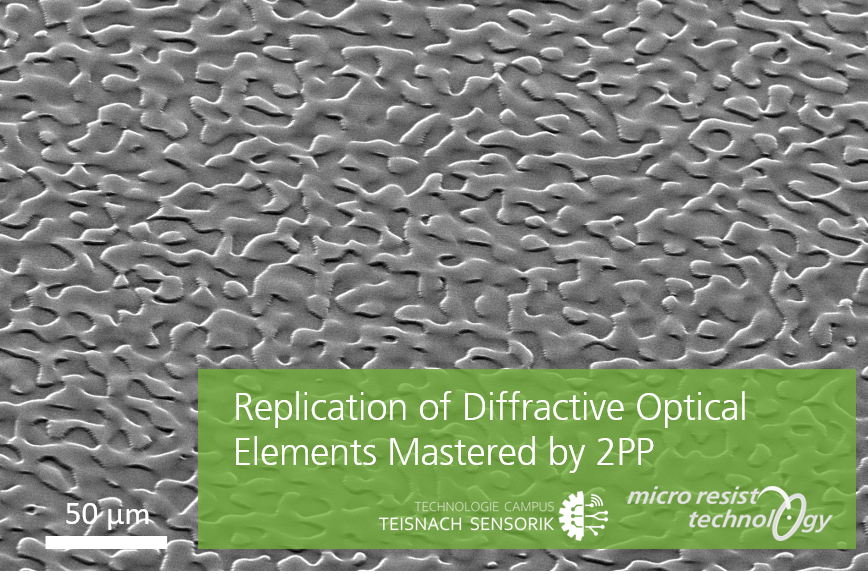
The demonstrated diffractive optical element (DOE) measures 3x3 mm² with a pixel size of 0.4x0.4 µm², displaying the TCTS campus logo in a 100 µm wide frame. It is designed for a 633 nm wavelength laser, with a structure height of 2-4 µm. The fabrication process includes using a single slice of varying height, with power calibration done just before fabrication and a writing speed of 2 mm/s and power of 35-50 mW.

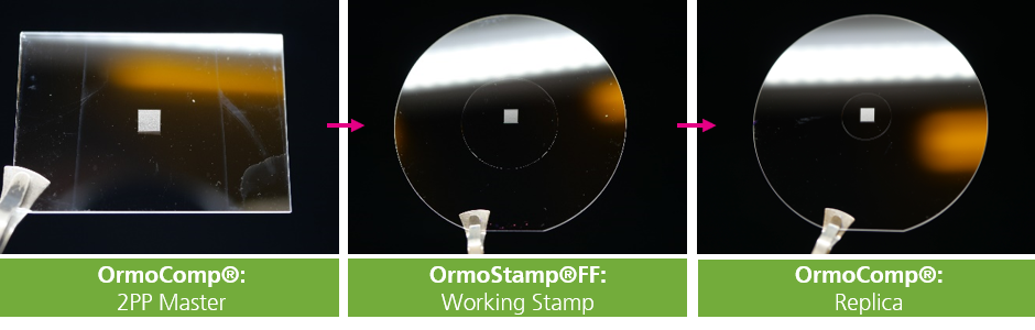
The replication process begins with coating the master with an antisticking layer (Video ASL deposition), crucial for smooth subsequent steps. Then, a stamp is made from OrmoStamp®FF, designed for high-fidelity replication. After another antisticking layer application, the replica is fabricated, ensuring consistent optical properties between master and replica.

Performance comparison

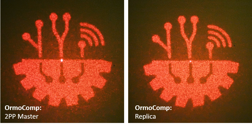
To validate the replication process, we compared the results using a 633 nm laser on both the master and the replica. The output was clear: the hologram from the replica closely matched that of the master, confirming that the process preserves the intricate details and optical characteristics of the original diffractive optical element.

In summary, the integration of 2PP mastering, nanoimprint, and OrmoComp® streamlines manufacturing and ensures high-quality results for modern optical applications.

Hybrid polymers
OrmoComp®
OrmoStamp®FF
2PP
DOE
Replication

Kontaktieren Sie uns.

Pflichtfelder sind mit einem * gekennzeichnet.
Element 32
0

Resist Alliance

micro resist technology is a single entry point for specialty chemicals used in micro and nano manufacturing in Europe. The portfolio of in-house products is complemented by the strategic sales of associated products that are manufactured by our international partners. Here we act as a high-service distributor and offer European medium-sized companies a wide range of complementary products from a single source, which can be used for both established and innovative production and manufacturing processes.

Kayaku Advanced Materials, Inc. (formerly MicroChem Corp.)

We offer photoresists and specialty chemicals for MEMS and microelectronic applications from our partner Kayaku Advanced Materials, with whom we have been working for more than 20 years.

DJ MicroLaminates, Inc.

We offer dry film resists for MEMS, microfluidics and packaging applications from our partner DJ MicroLaminates, with whom we have been cooperating for over two years.

Dry Films

Dry films are ready-to-use polymer films as laminate foil with a high accuracy of the film thickness and excellent adhesion behaviour on various substrates. They are very simple in handling, photo-structurable and both as cut sheets and as roll material available.

  • Available in different film thicknesses
  • UV-crosslinking as negative photoresist
  • Feasibility of high aspect ratios
  • Vertical sidewalls
  • Multi lamination possible – up to 6 layer  complex multi-layer designs
  • High chemical resilience


  • Application as permanent material for optical application (e.g. lenses, wave guides …), in micro fluidics

Functional materials for inkjet-printing

Special designed functional materials from the product groups Hybrid Polymers, Photoresists, and Nanoimprint Polymers for the deposition and alternative patterning using inkjet printing process

  • Available in different viscosities (adjustable)
  • Suitable in commercial inkjet printing devices
  • Focused on high reliability of droplet generation
  • UV-curable formulations


  • Usable as a permanent material for optical application (e.g. lenses, wave guides, optical couplers, diffractive elements, …)
  • Packaging material in the micro electronic
  • Deposition / patterning on substrates with surface topography
  • Imprint material for nano-structuring with high dose accuracy

Nanoimprint Resists

Nanoimprint Lithography (NIL) is a straight forward, low cost, and high throughput capable technology for the fabrication of nanometer scaled patterns. Main application fields are photonics, next generation electronics, as well as bio- and sensor applications.

micro resist technology GmbH has provided tailor-made resist formulations for nanoimprint lithography (NIL) since 1999. The unique key features of our products are outstanding film forming and imprinting performance beside excellent pattern fidelity and plasma etch stability. Besides our highly innovative material developments in close contact to industrial needs, our strength is the ability to adjust our materials in film thickness as well as addressing certain needs of the specific use cases within the formulation. Our nanoimprint resists are mostly applied as an etch mask for pattern transfer into various substrates, like Si, SiO2, Al or sapphire.

Our portfolio covers materials for the classical thermal NIL (T-NIL), in which a thermoplastic polymer is used, as well as UV-NIL, in which a liquid formulation is photo crosslinked upon photo exposure. With our technological expertise and know-how we are able to find the right material for your process and applications. Please contact us for your technical support!

Hybrid Polymers

micro resist technology offers a broad portfolio of UV-curable hybrid polymer products for micro-optical applications. Their excellent optical transparency and high thermal stability makes them perfectly suitable for the production of polymer-based optical components and waveguides. The main fields of application are micro lenses, diffractive optical elements (DOE), gratings, and single-mode or multi-mode waveguides.

OrmoComp®: DE 30 210 075 433; IR 1 091 982 ; TW 100030626; OrmoClear®: DE 30 210 075 434; IR 1 091 359 ; TW 100030628; OrmoStamp®: DE 30 210 075 435; IR 1 092 621 ; TW 100030629; OrmoPrime®: DE 30 210 075 436

Positive Photoresists

Positive Photoresists for UV lithography (mask aligner, laser, greyscale exposure) and e-beam lithography

  • Variety of viscosities for 0.1 µm – 60 µm film thickness in one spin-coating step
  • Effective for broadband, g-line, h-line or i-line exposure, laser direct writing at 350…450 nm and e-beam lithography
  • No post exposure bake
  • Easy removal
     
  • For pattern transfer: Etch mask, mould for electroplating, mould for UV moulding
  • Use in microsystems technology, microelectronics, micro-optics – manufacture of e.g. MEMS, LEDs, ICs, MOEMS, fiber optics telecommunications devices, flat panel displays

Negative Photoresists

Photoresists for UV (mask aligner, laser)/ DUV and e-beam lithography

  • Effective for broadband and i-line, Deep UV, e-beam exposure, or laser direct writing @ 405 nm
  • Lift-off resists with tunable pattern profile, high temperature stability up to 160 °C
  • Variety of viscosities for different film thicknesses in one spin-coating step
     
  • For pattern transfer: Physical vapour deposition (PVD) and single  layer lift-off, etch mask, mould for electroplating
  • For permanent applications: Polymeric waveguides
  • Use in microsystems technology, microelectronics, micro-optics  – manufacture of e.g. LEDs, ICs, MEMS, flat panel displays, fiber optics telecommunications devices