Element 2
+49 30 641 670 100
Element 1
info@microresist.de
TOKKachel2x3
+++ Company Announcement +++
Information

micro resist technology GmbH becomes part of the TOK Group for joint expansion into European semiconductor manufacturing and related markets


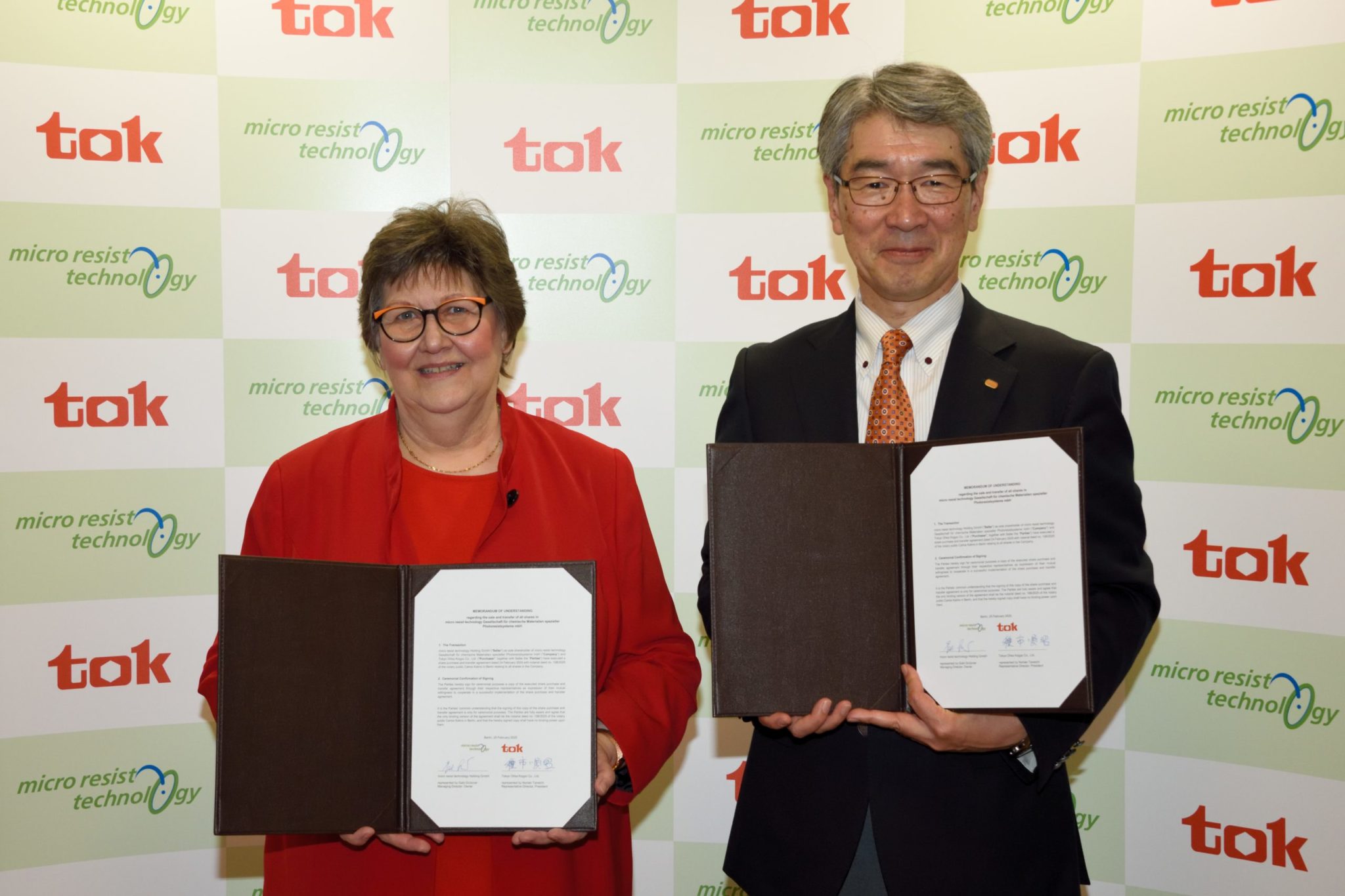
Berlin (Germany), May 5th 2025 - We are excited to announce that micro resist technology GmbH (MRT), headquartered in Berlin (Germany), has signed a formal purchase agreement with TOKYO OKHA KOGYO CO., LTD. (TOK), headquartered in Kanagawa (Japan), on 24th February 2025 to join the TOK Group through full acquisition.  The signing ceremony took place at MRT in Berlin with Mrs. Gabi Grützner, Founder of MRT, and Mr. Noriaki Taneichi, Representative Director, President & Chief Executive Officer of TOK.

The strategic acquisition brings together two established photoresist developers and manufacturers as committed partners to create new corporate values through the fusion of both companies and thus further strengthen their customer-oriented business approaches. The cooperation is starting at a favorable time, as Europe becomes increasingly important as a semiconductor production location for the local user industry. TOK further expands its businesses to the semiconductor industry in Europe. MRT further intensifies its global reach of business opportunities through the worldwide presence of TOK group and making European material innovations available to an expanded list of customers and complementary fields of application and industry level.

While TOK Europe Branch will continue to be responsible for selling TOK's existing product portfolio in Europe, MRT continues its operation under its known corporate brand with no interruption towards its customers and supplying partner companies.

“It is with a view to the future of the company that I founded 32 years ago that I am handing it over to a strong strategic partner in the photoresist business. micro resist technology GmbH has been intensively involved in the research and sale of innovative photoresists and photopolymers for three decades and we have now found a strategic partner in this innovative resist business field that has been pursuing the same corporate philosophy for many decades as the world's leading materials supplier to the global semiconductor industry. We are thus combining our innovative strength with the necessary large-scale industrial experience of our partner in order to market European photoresist innovations worldwide,” says Mrs. Gabi Grützner, Founder of MRT.

“We are very pleased to welcome MRT to the TOK group. We are confident that we will be able to contribute to a sustainable future through chemistry better than ever before with a combination of MRT’s innovative technologies in electronic and optical materials and our technologies we have cultivated since our founding,” concludes Mr. Noriaki Taneichi, President of TOK.


About micro resist technology GmbH

MRT is a leading company in the development and production of innovative photoresists, polymers and photopolymers as well as complementary process chemicals for lithographic manufacturing processes in micro- and nanostructuring. The products are used in key technologies and growth markets such as microsystems technology, microelectronics, optoelectronics, micro- and nanophotonics, micro- and nanotechnology as well as the life sciences. Since its foundation in 1993 MRT has build up strong technological capabilities as a research and development-driven company with solid relationships to European customers that uses microfabrication as well as leading research institutions worldwide. The acquisition is also a decisive strategic step for the company to secure the succession of the owner.

Website: https://www.microresist.com


About TOKYO OHKA KOGYO CO., LTD.

TOK is a renown global chemical manufacturer that provides microprocessing materials such as photoresists that play a key role in the semiconductor manufacturing process. TOK was founded as a high-purity chemical manufacturer in 1940 and entered semiconductor materials field in late 1960s, currently supplying the leading semiconductor manufacturing field utilizing the world’s most advanced microprocessing technology. As long-established photoresist manufacturer, TOK strives to contribute to the development of society. The acquisition is part of the seven key strategies set out in “tok Medium-Term Plan 2027” launched in 2025 toward the realization of tok Vision 2030.

Website: https://www.tok.co.jp/eng


Note: This announcement was published on May 5th, 2025, after all legal details have been officially confirmed.

Contact us:

Fields marked with an * are required.
Element 32
0

Resist Alliance

micro resist technology is a single entry point for specialty chemicals used in micro and nano manufacturing in Europe. The portfolio of in-house products is complemented by the strategic sales of associated products that are manufactured by our international partners. Here we act as a high-service distributor and offer European medium-sized companies a wide range of complementary products from a single source, which can be used for both established and innovative production and manufacturing processes.

DuPont Electronic Solutions (formerly DOW Electronic Materials / Rohm and Haas Europe Trading ApS)

We offer products for semiconductor technologies, advanced packaging and dry film resists from our partner DuPont, with whom we have been working for more than 20 years.

Kayaku Advanced Materials, Inc. (formerly MicroChem Corp.)

We offer photoresists and specialty chemicals for MEMS and microelectronic applications from our partner Kayaku Advanced Materials, with whom we have been working for more than 20 years.

DJ MicroLaminates, Inc.

We offer dry film resists for MEMS, microfluidics and packaging applications from our partner DJ MicroLaminates, with whom we have been cooperating for over two years.

Dry Films

Dry films are ready-to-use polymer films as laminate foil with a high accuracy of the film thickness and excellent adhesion behaviour on various substrates. They are very simple in handling, photo-structurable and both as cut sheets and as roll material available.

  • Available in different film thicknesses
  • UV-crosslinking as negative photoresist
  • Feasibility of high aspect ratios
  • Vertical sidewalls
  • Multi lamination possible – up to 6 layer  complex multi-layer designs
  • High chemical resilience


  • Application as permanent material for optical application (e.g. lenses, wave guides …), in micro fluidics

Functional materials for inkjet-printing

Special designed functional materials from the product groups Hybrid Polymers, Photoresists, and Nanoimprint Polymers for the deposition and alternative patterning using inkjet printing process

  • Available in different viscosities (adjustable)
  • Suitable in commercial inkjet printing devices
  • Focused on high reliability of droplet generation
  • UV-curable formulations


  • Usable as a permanent material for optical application (e.g. lenses, wave guides, optical couplers, diffractive elements, …)
  • Packaging material in the micro electronic
  • Deposition / patterning on substrates with surface topography
  • Imprint material for nano-structuring with high dose accuracy

Nanoimprint Resists

Nanoimprint Lithography (NIL) is a straight forward, low cost, and high throughput capable technology for the fabrication of nanometer scaled patterns. Main application fields are photonics, next generation electronics, as well as bio- and sensor applications.

micro resist technology GmbH has provided tailor-made resist formulations for nanoimprint lithography (NIL) since 1999. The unique key features of our products are outstanding film forming and imprinting performance beside excellent pattern fidelity and plasma etch stability. Besides our highly innovative material developments in close contact to industrial needs, our strength is the ability to adjust our materials in film thickness as well as addressing certain needs of the specific use cases within the formulation. Our nanoimprint resists are mostly applied as an etch mask for pattern transfer into various substrates, like Si, SiO2, Al or sapphire.

Our portfolio covers materials for the classical thermal NIL (T-NIL), in which a thermoplastic polymer is used, as well as UV-NIL, in which a liquid formulation is photo crosslinked upon photo exposure. With our technological expertise and know-how we are able to find the right material for your process and applications. Please contact us for your technical support!

Hybrid Polymers

micro resist technology offers a broad portfolio of UV-curable hybrid polymer products for micro-optical applications. Their excellent optical transparency and high thermal stability makes them perfectly suitable for the production of polymer-based optical components and waveguides. The main fields of application are micro lenses, diffractive optical elements (DOE), gratings, and single-mode or multi-mode waveguides.

OrmoComp®: DE 30 210 075 433; IR 1 091 982 ; TW 100030626; OrmoClear®: DE 30 210 075 434; IR 1 091 359 ; TW 100030628; OrmoStamp®: DE 30 210 075 435; IR 1 092 621 ; TW 100030629; OrmoPrime®: DE 30 210 075 436

Positive Photoresists

Positive Photoresists for UV lithography (mask aligner, laser, greyscale exposure) and e-beam lithography

  • Variety of viscosities for 0.1 µm – 60 µm film thickness in one spin-coating step
  • Effective for broadband, g-line, h-line or i-line exposure, laser direct writing at 350…450 nm and e-beam lithography
  • No post exposure bake
  • Easy removal
     
  • For pattern transfer: Etch mask, mould for electroplating, mould for UV moulding
  • Use in microsystems technology, microelectronics, micro-optics – manufacture of e.g. MEMS, LEDs, ICs, MOEMS, fiber optics telecommunications devices, flat panel displays

Negative Photoresists

Photoresists for UV (mask aligner, laser)/ DUV and e-beam lithography

  • Effective for broadband and i-line, Deep UV, e-beam exposure, or laser direct writing @ 405 nm
  • Lift-off resists with tunable pattern profile, high temperature stability up to 160 °C
  • Variety of viscosities for different film thicknesses in one spin-coating step
     
  • For pattern transfer: Physical vapour deposition (PVD) and single  layer lift-off, etch mask, mould for electroplating
  • For permanent applications: Polymeric waveguides
  • Use in microsystems technology, microelectronics, micro-optics  – manufacture of e.g. LEDs, ICs, MEMS, flat panel displays, fiber optics telecommunications devices