


“Innovation distinguishes between a leader and a follower.” (Steve Jobs)
Innovation is our source, regardless of whether driven by our self or by our customers. We claim to take the lead with our products and innovative solutions. To reach this goal, a close interaction between research and development is essential. In our research projects we work closely with scientific institutions all over the world. Because only who is well connected will be successful on the top. In the development the focus is on the customer and his requirements. The tighter the bonding is the more tailored solutions we can generate. Together with the customer, we are able to recognize, evaluate and implement the needs for tomorrow today. The brilliancy can always be seen in the simplicity, especially related to the customer. Our solutions should clearly bring added value to customers. This creates mutual trust, the basis for a long-term cooperation.
“The projects Copysphär and Reflex are co-financed by the European Regional Development Fund (ERDF).”
![]()
Projectnr.: 10169159
Funding agency: State of Berlin
Term of Project: 01.04.2020 – 31.12.2022
Project goal
A new technology is under development for the replication of diffraction optics on curved substrates. Reflective zone plates combine the functions of a mirror and a grating and thus avoid losses in light intensity. Zone plates cover a wide wavelength range from the infrared to soft X-rays and are used in spectrometers in many fields such as research, optical characterization, geology, biology, agriculture, medical technology, etc.
In order to realize high precision during pattern transfer, different technologies for generating pre-forms and replications will be developed for strongly bent surfaces. High precision adjustment systems are necessary for the pattern transfer as well as for the deforming step of stamp and replica after the process.
Project benefits
The Copysphär project aims at the development of all processes in order to achieve an integrated value chain in the commercial production of reflection zone plates for the market. These new components, which allow both energy dispersion and focusing, are primarily intended to supply the market for optical measuring devices for analysis (spectrometers, monochromators).
Outlook
With the development of a practice-relevant, efficient replication process, micro resist technology GmbH shows the high technical level of replication technology in-house. It also opens up another new market for the company to use its innovative, optical materials, hybrid polymers.
“This project is co-financed by the European Regional Development Fund (ERDF).”
![]()
Projectnr.: H2020-IND-CE-2016-17/H2020-NMBP-PILOTS-2017, 760915
Funding agency: Europäische Union
Term of Project: 01.01.2018 – 31.12.2021
Projectwebsite: http://www.sunpilot.eu/
Project number: 10162951
Funding agency: State of Berlin
Term of project: 01.01.2017 – 31.05.2020
Project goal
The project is the first to research industrial production of reflection zone plates (RZP) worldwide. The biggest scientific and technical challenge for the project is that the diffractive optical high-tech elements have to be individually designed in a complex process. The innovation in this project is the development of an inexpensive replication process in order to finally make this RZP available to the market for efficient use in optical analysis. The three participating institutions (Neutron Optics Berlin NOB GmbH, Institute for Applied Photonics e.V. IAP, micro resist technology GmbH MRT) are researching new technologies and possible applications for the production of RZP. In addition, adapted measuring technology processes must be researched and developed in order to control the quality in the RZP production and to characterize properties such as the surface roughness, the reflectivity and the structural fidelity of the RZP.
Project benefits
The REFLEX project aims at the development of all processes in order to achieve an integrated value chain in the commercial production of reflection zone plates for the market. To date, these diffractive optical elements, which are characterized by high flexibility, high light output and high time resolution, have only been produced by research institutes. These new components, which allow both energy dispersion and focusing, are primarily intended to supply the market for optical measuring devices for analysis (spectrometers, monochromators).
outlook
With the development of a practice-relevant, efficient replication process, micro resist technology GmbH shows the high technical level of replication technology in-house. It also opens up another new market for the company to use its innovative, optical materials, hybrid polymers.
“This project is co-financed by the European Regional Development Fund (ERDF).”
![]()
Programmträger: BMBF
Projekte:
Projektnr.: 03ZZ0111E
Projektlaufzeit: 01.07.2015 – 31.12.2016
Projektnr.: 03ZZ0125F
Projektlaufzeit: 01.11.2016 – 31.10.2019
Projektnr.: 03ZZ0124C
Projektlaufzeit: 01.09.2016 – 31.12.2019
Projektwebseite: www.advanced-uv.de/fe-projekte/
Projectnr.: 03WKCT1D
Funding agency:Funding agency:BMBF
Term of Project: 01.09.2016 – 31.08.2019
Projectwebsite: http://www.polyphotonics-berlin.de/projekte/
Projektnr.: 03WKCT1D
Programmträger: BMBF
Projektlaufzeit: 01.09.2016 – 31.08.2019
Projektwebseite: http://www.polyphotonics-berlin.de/projekte/
Projektnr.: 604668
Programmträger: European Commission FP7
Projektlaufzeit: 01.12.2013 – 30.11.2017
Projektziele
The QUANTIHEAT project tackles issues related to thermal metrology at the nanoscale and aims at delivering validated standards, methods and modeling tools for nanothermal designs and measurements. This 4-year project brought together 20 partners from 9 different countries. It has received funding from the EU 7th FP for research, technological development and demonstration (FP7/2007-2013) under grant agreement n°604668.
The collaboration of some partners originally began with a CNRS-supported network dealing with micro and nanoscale heat transfer. Measurement by Scanning Thermal Microscopy (SThM) was one of its targets and a think tank was constituted at the French level in 2007 on this topic. This subsequently became part of a larger-scale CNRS-supported network ‘Thermal nanoscience and nanoengineering’ in which there was an Advanced Metrologies group with 8 European partners. This group intended to widen its participation to the European level, and was willing to extend more opportunities for the exchange of scientific ideas as well as metrology expertise and disseminating the results to the European industry (SMEs and large companies). The QUANTIHEAT project was born in this context, bringing together 20 partners with complementary technical skills and scientific expertise required for the successful execution of the project.
Outcome and major results
_1) THERMAL NIL RESIST FORMULATIONS: Only analytical methods like SThM can provide the local thermo-physical investigations needed for nanoscaled polymer structures in an appropriate fashion. In QUANTIHEAT, for both applications of thermal (T)-NIL and UV-NIL, thermal and thermomechanical measurements with AFM and SThM were performed on test samples in which polymers are in confined dimensions with tailored molecular architecture. Samples, differing in terms of molecular weight among other parameters and obtained by applying different imprint conditions, were studied in order to have a direct feedback from imprinted structures and not just from the bulk material. Special attention was paid to tailored fluorinated additives (admixed to the resist formulation) that strongly facilitate the demolding step in the NIL process. MRT focused on the development of such new fluorinated additives for use in thermal NIL resist formulations. Their performance was evaluated by thin film and imprint studies. MRT prepared various thin NIL resist films and imprints (film thicknesses of 200 nm, 100 nm and sub-100 nm) using reference stamps featuring different types of micro- and nanostructures for different thermal and photo-curable NIL resists. The performed SThM measurements provided valuable information − particularly in terms of the evaluation of the apparent glass transition temperatures (Tg’s) of the different films finally prepared with different NIL resist versions. The performed work strongly expanded MRTs knowledge on structure-property-relationships of additives, so that new design rules regarding the composition and the architecture of fluorinated additives could be derived and established. Generally, the newly developed technology of fluorinated additives admixed to NIL resist formulations greatly improves the imprint performance of the NIL resists leading thus to a drastically lower defectivity rate which is a key metric for most industrial high-volume fabrication processes. These results were the basis for acquiring and participating in a pilot line project in which the material production will be scaled up from lab scale to volumes relevant for industrial applications.
_2) EVALUATION OF NIL RESISTS FOR A USE IN AREA-SELECTIVE (AS)-ALD: Thermal and thermo-mechanical aspects typically have a great impact not only on the processing of (thermal) NIL resists but also on the performance in post-processing techniques like the pattern transfer via anisotropic plasma etching or subsequent modifications by e.g. ALD-based techniques. The combination of NIL with ALD is rather promising as it opens up completely new applications and addresses current challenges in the field of nanotechnology. Especially the controlled deposition of thin film inorganic materials via ALD on pre-defined areas, the so-called area-selective (AS)-ALD requires special strategies. In this regard, we have devised a multi-step process depicted in Figure 1 which seems highly suited for the evaluation of potential combinations between NIL and ALD.
To this end, in a first step an organic UV-NIL resist like mr-NIL210 is imprinted by using a PDMS-based stamp. The imprint itself is conducted in such a way, that the cavities of the stamp are only partially filled so that the residual layer of the imprinted pattern is already minimized. However, in order to fully remove the very thin residual layer of the NIL resist a wet-chemical development applying an efficient solvent like acetone was carried out. Due to the slight oxygen sensitivity of the mr-NIL210 material the partially cured but not fully cross-linked residual layer featuring a few nanometers thickness remains still soluble after the UV-illumination step and can therefore be removed by an appropriate solvent. Likewise, the thin adhesion promoting layer based on soluble UL1 material is removed by another wet-chemical developing step applying e.g. isopropanol as solvent. The obtained patterns were then subjected to different ALD processes resulting in the growth of various inorganic materials like e.g. Al2O3, ZnO, TiO2, ZrO2, Pt, HfO2, Ta2O5, respectively. Ideally, the inorganic material is selectively deposited only at those areas that feature the bare substrate surface whereas no growth takes place onto the NIL resist patterns. By performing a subsequent oxygen plasma step, the fully organic NIL material of mr-NIL210 can then be then removed so that only the patterns of the ALD processed materials are left over.

Fig. 1: Schematic illustration of the different subsequent processing steps performed to evaluate useful combinations between NIL and area-selective ALD processes.
In general, the analysis of the performed studies clearly indicate that ALD and NIL are highly complementary techniques particularly due to the topographic profile / relief of imprinted NIL resist patterns, so that often no absolute area-selectivity performance is needed for specific applications. A high or partial area-selectivity performance is sometimes already sufficient. Importantly, obtained results suggest that for a couple of potential applications no absolute area-selectivity performance is required or necessary. In addition, the topographic profile of an imprinted structure can be highly advantageous in terms of the fabrication of specific patterns that cannot be equally achieved by other patterning techniques as can be seen exemplarily in the formation of ring-like patterns displayed in Figure 2 (AFM pictures on the right).
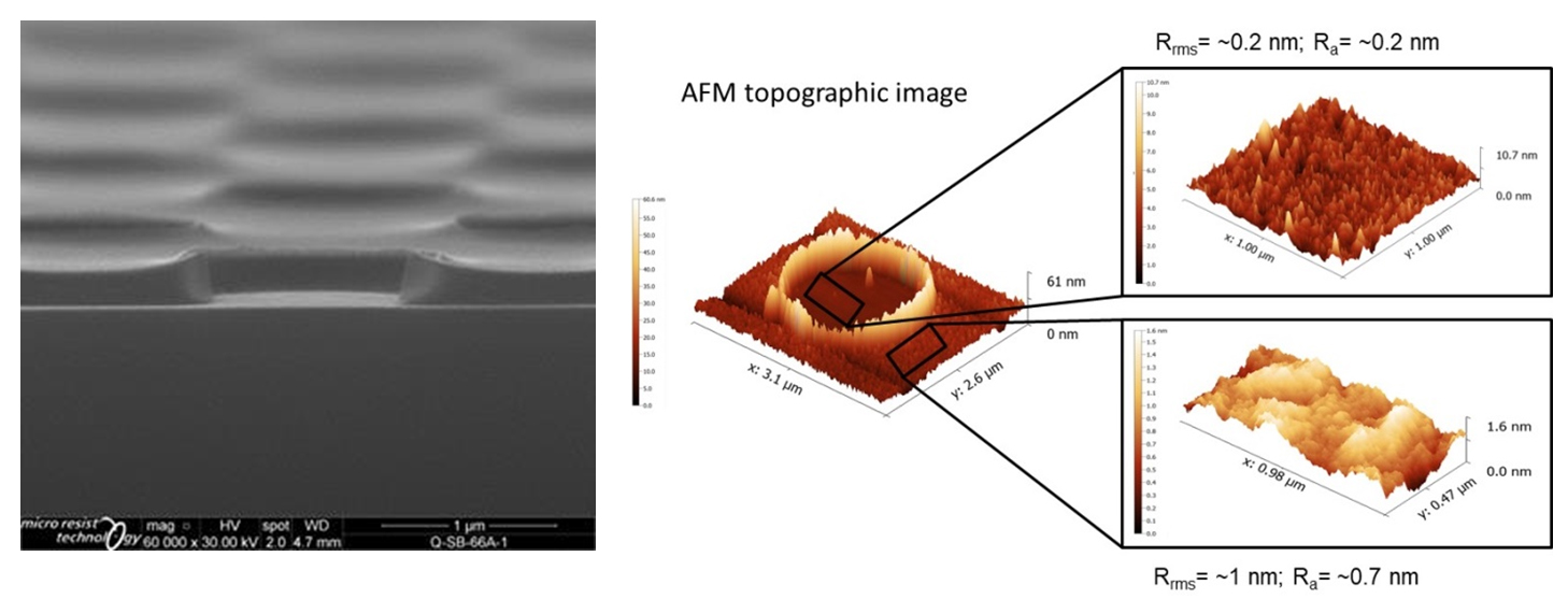
Fig. 2: Exemplary SEM image of the precursor scaffold structure prepared via UV-imprinting of mr-NIL210 and subsequent wet-chemical developing steps (on the left) and AFM analyses (roughness and topography) of a ring-like pattern (on the right) obtained after performing an ALD process (of ZnO) and a subsequent oxygen plasma etching step to remove remaining organic NIL resist material.
_3) NIL STAMP COATINGS VIA ALD PROCESS: AFM and SThM results clearly indicated that the preparation of thin ALD deposited Al2O3 layers onto imprinted mr-NIL210 patterns and the subsequent preparation of different anti-sticking layers onto the Al2O3 layers render these systems potentially useful as thermally and mechanically robust NIL working stamps. The SThM measurements further contributed to valuable feedback by evaluating the thermal characteristics thus verifying the required thermal robustness of the ALD-coated NIL stamps. Due to the general nature of this technology such kind of systems could also be transferred to other application fields − particularly for permanent applications where (imprinted) patterns are exposed to harsh conditions such as heat and/or a corrosive environment or when a defined surface modification is required which is the case for different life-science applications.
In conclusion, the QUANTIHEAT project enabled an increase of industrial competitiveness for MRT through strengthened capabilities in innovative products and services: these include custom tailored UV- and T-NIL products, know-how about product formulation developed during the project and properties, as well as the combination of NIL to other nanotechnology processes like ALD and the potential of such technology conjunctions to open up new possible applications.
Publications and dissemination:
You are currently viewing a placeholder content from Vimeo. To access the actual content, click the button below. Please note that doing so will share data with third-party providers.
More InformationYou are currently viewing a placeholder content from YouTube. To access the actual content, click the button below. Please note that doing so will share data with third-party providers.
More InformationYou need to load content from reCAPTCHA to submit the form. Please note that doing so will share data with third-party providers.
More InformationYou need to load content from reCAPTCHA to submit the form. Please note that doing so will share data with third-party providers.
More InformationYou are currently viewing a placeholder content from Google Maps. To access the actual content, click the button below. Please note that doing so will share data with third-party providers.
More InformationYou are currently viewing a placeholder content from Google Maps. To access the actual content, click the button below. Please note that doing so will share data with third-party providers.
More InformationYou are currently viewing a placeholder content from Mapbox. To access the actual content, click the button below. Please note that doing so will share data with third-party providers.
More InformationYou are currently viewing a placeholder content from OpenStreetMap. To access the actual content, click the button below. Please note that doing so will share data with third-party providers.
More Information